Display substrate, preparation method thereof and display device
A display substrate and modulation layer technology, which is applied in semiconductor/solid-state device manufacturing, organic semiconductor devices, semiconductor devices, etc., can solve problems such as high color gamut, high brightness, and difficulty in obtaining silicon-based OLED microdisplays
- Summary
- Abstract
- Description
- Claims
- Application Information
AI Technical Summary
Problems solved by technology
Method used
Image

Examples
no. 1 example
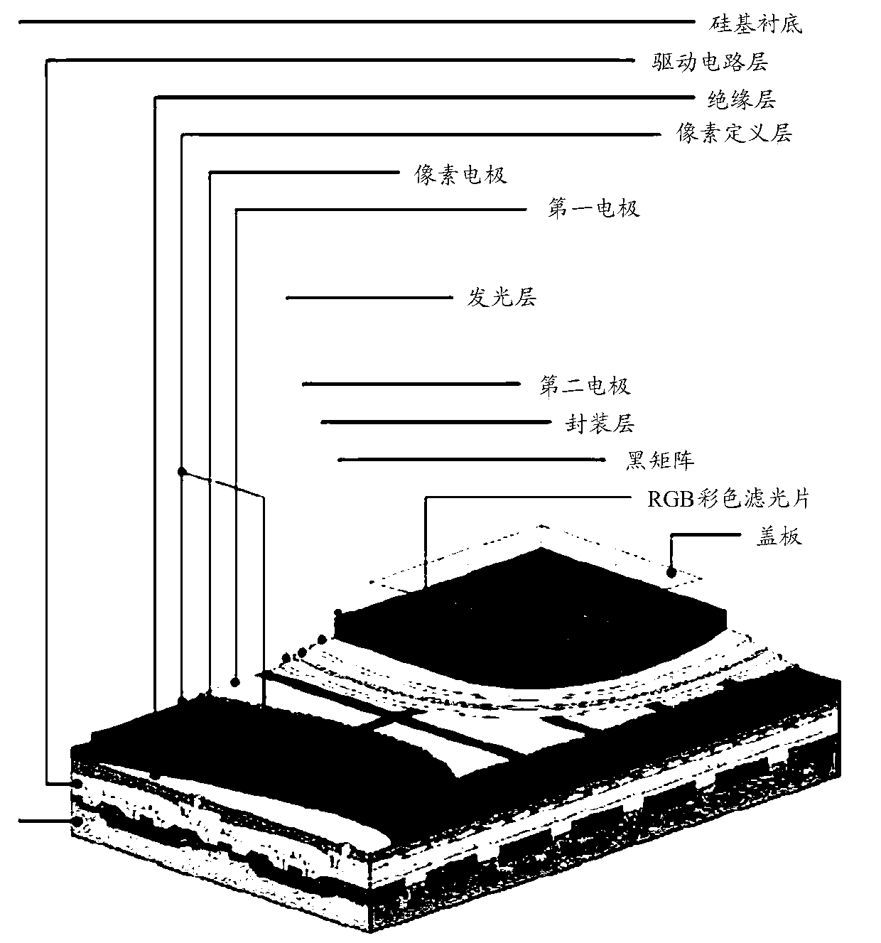
[0108] First, the technical solution of this embodiment is described through the preparation process of the display substrate of this embodiment. The "patterning process" referred to in this embodiment includes treatments such as film deposition, photoresist coating, mask exposure, development, etching, and photoresist stripping, which are mature preparation processes in related technologies. The deposition may use known processes such as sputtering, evaporation, and chemical vapor deposition, the coating may use a known coating process, and the etching may use a known method, which is not specifically limited herein. In the description of this embodiment, it should be understood that “thin film” refers to a thin film made by depositing or coating a certain material on a substrate. If the "thin film" does not require a patterning process or photolithography process during the entire production process, the "thin film" can also be called a "layer". If the "thin film" needs a pa...
no. 2 example
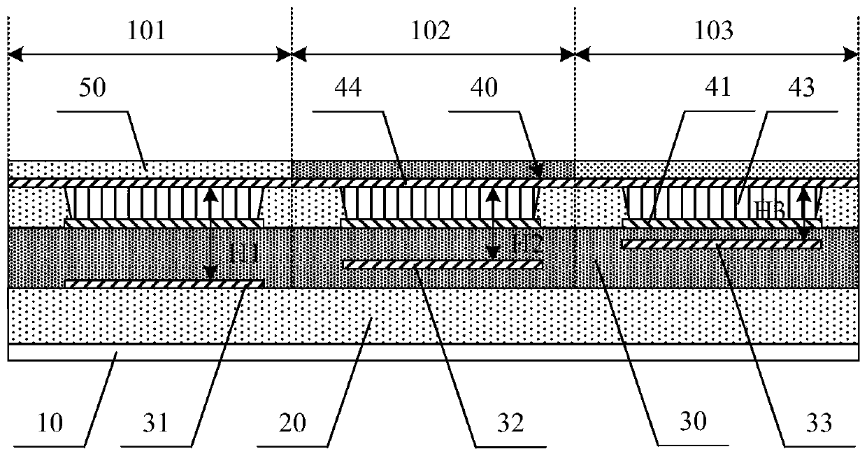
[0154] Figure 18 It is a schematic structural view of the second embodiment of the display substrate of the present invention. This embodiment is an extension of the foregoing first embodiment, and the main structure of the display substrate is basically the same as the foregoing first embodiment. Such as Figure 18 As shown, the difference is that the third connection block is not provided in the fourth via hole K4 of each sub-pixel, and the first electrode 41 of the light-emitting structure layer of the first sub-pixel 101 passes through the fourth modulation layer 38 opened on the The via hole K4 is directly connected to the second connecting block 37 of the sub-pixel, the first electrode 41 of the second sub-pixel 102 is directly connected to the second connecting block 37 of the sub-pixel through the fourth via hole K4, and the third sub-pixel 103 is An electrode 41 is directly connected to the third reflective electrode 33 of the sub-pixel through the fourth via hole K4....
no. 3 example
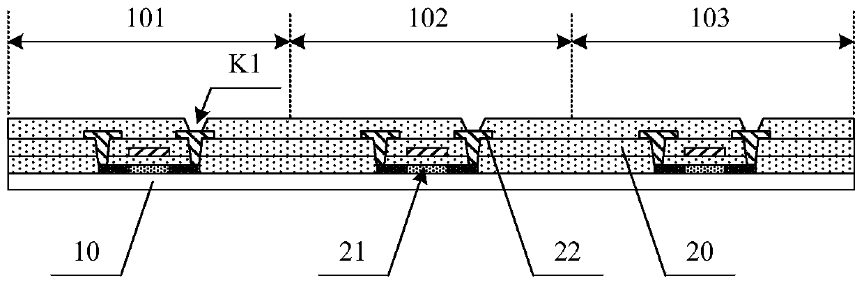
[0158] Figure 19 It is a schematic structural view of the third embodiment of the display substrate of the present invention. This embodiment is an extension of the foregoing first or second embodiment. Such as Figure 19 As shown, the display substrate of this embodiment includes a display area and a frame area. The main structure of the display area is the same as that of the foregoing first or second embodiment. The frame area includes a lead structure layer, and the lead structure layer includes a lead pad 60. The lead pad 60 and the drain electrode 22 of the driving transistor 21 are arranged in the same layer, and are formed by the same patterning process. The lead structure layer is covered with a first modulation layer 34, a second modulation layer 36 and a third modulation layer 38, and a lead via hole exposing the lead pad 60 is opened on the modulation layer.
[0159] This embodiment shows that the preparation process of the substrate is basically the same as that of...
PUM
 Abstract
Description
Claims
Application Information
 - R&D
- Intellectual Property
- Life Sciences
- Materials
- Tech Scout
- Unparalleled Data Quality
- Higher Quality Content
- 60% Fewer Hallucinations
Browse by: Latest US Patents, China's latest patents, Technical Efficacy Thesaurus, Application Domain, Technology Topic, Popular Technical Reports.
© 2025 PatSnap. All rights reserved.Legal|Privacy policy|Modern Slavery Act Transparency Statement|Sitemap|About US| Contact US: help@patsnap.com