Flexible nanofiber zinc tin oxide field effect transistor and preparation method thereof

A field effect transistor and nanofiber technology, applied in the field of microelectronics, can solve the problems of hindering the development of NF process, difficult to control fiber distribution, high process cost, etc., to achieve large-scale industrial application, good application potential, high mobility. Effect

Pending Publication Date: 2019-12-03
XIAN JIAOTONG LIVERPOOL UNIV
View PDF0 Cites 4 Cited by
  • Summary
  • Abstract
  • Description
  • Claims
  • Application Information

AI Technical Summary

Problems solved by technology

However, traditional processes for preparing NF, such as: electrospinning, evaporation, magnetron, and nano-combing, etc., all have certain defects, such as: difficult to control fiber distribution, high substrate requirements, high process costs, etc.
On the other hand, traditional organic NF semiconductor materials often have low mobility and high toxicity, which also hinders the development of NF technology.

Method used


Image

  • Flexible nanofiber zinc tin oxide field effect transistor and preparation method thereof
  • Flexible nanofiber zinc tin oxide field effect transistor and preparation method thereof

Examples


Embodiment

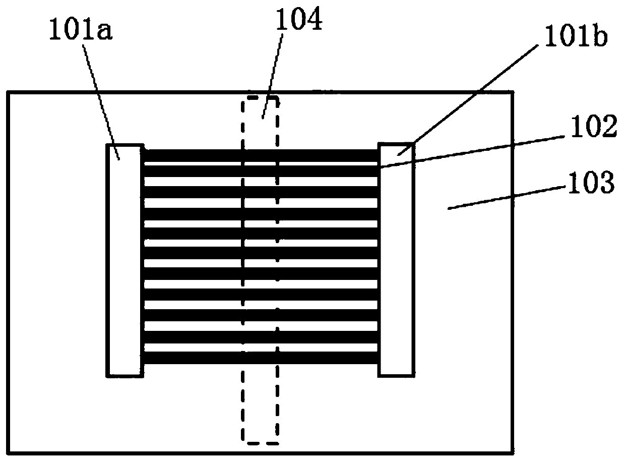
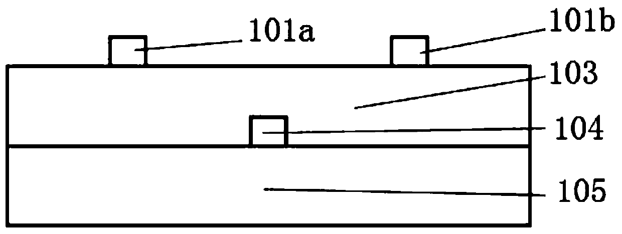
[0038] as attached Figure 1-2 As shown, a field effect transistor of flexible nanofiber zinc tin oxide includes a top source electrode layer 101a, a top drain electrode layer 101b arranged from top to bottom, a carrier channel layer 102 of a nanofiber structure, and a dielectric layer 103 , a bottom gate electrode layer 104 and a substrate 105; the carrier channel layer 102 of the nanofibrous structure is a cluster of zinc tin oxide (ZTO) filaments with a diameter of about 100-300 nm prepared by a sol method, with a uniform number, The advantage of neat direction. The top source electrode layer 101a, the top drain electrode layer 101b and the bottom gate electrode layer 104 are transparent indium tin oxide (ITO) electrodes made by an aqueous solution method with a thickness of 50-150 nm and a channel width-to-length ratio of 10-20 (The channel width-to-length ratio is a dimension between a pair of source-drain electrodes), and the specific value is determined by the mask pla...


PUM


Abstract

The invention discloses a flexible nanofiber zinc tin oxide field effect transistor and a preparation method thereof. The flexible nanofiber zinc tin oxide field effect transistor comprises a top source electrode layer, a top drain electrode layer, a carrier channel layer of a nanofiber structure, a dielectric layer, a bottom gate electrode layer and a substrate which are arranged from top to bottom, wherein the carrier channel layer of the nanofiber structure is a zinc tin oxide filament cluster which is prepared by a sol method and has the diameter of about 100-300 nm. The preparation methodcomprises the following steps of: a) cleaning the substrate; b) preparing the bottom gate electrode layer, c) preparing a hafnium oxide dielectric layer, d) preparing a carrier channel layer with a nanofiber structure, and e) preparing a top source electrode layer and a top drain electrode layer. According to the scheme, the nanofiber (NF) filaments are prepared by adopting a sol method, the operation is simple and convenient, the distribution and direction are easy to control, the cost is low, the uniformity is relatively high, and large-scale industrial application can be realized; the advantages of environmental protection, high mobility and the like are achieved; the method can be applied to the field of flexible wearable circuits; and the whole device is transparent, and has good application potential in the optical field.

Description

technical field [0001] The invention relates to the technical field of microelectronics, in particular to a flexible nanofiber zinc-tin oxide field-effect transistor and a preparation process based on a sol method. Background technique [0002] In recent years, with the increasing demand for advanced electronic devices, field-effect transistor (FET) devices have gradually attracted a lot of research and are regarded as one of the most critical basic devices in modern electronic device applications. . [0003] One-dimensional nanostructured devices, such as nanofibers (NFs), etc., are currently Has been called a research hotspot. The NF structure FET channel layer is one or several fibrous semiconductor nano-filaments, which can effectively reduce the scattering of carriers and form an effective conductive channel compared with the traditional thin-film structure FET. However, the traditional processes for preparing NF, such as: electrospinning, evaporation, magnetron, and...

Claims


Application Information

Patent Timeline
Patent Type & Authority Applications(China)
IPC IPC(8): H01L29/775H01L21/335
CPCH01L29/66439H01L29/775
Inventor 赵天石赵春赵策洲杨莉于水长
Owner XIAN JIAOTONG LIVERPOOL UNIV
Why Eureka
Try Eureka