Wide-spectrum self-driven inorganic perovskite photoelectric detector and preparation method thereof
A photodetector and perovskite technology, applied in the field of photodetectors, can solve the problems of insufficient response range of perovskite materials, limited development, poor stability of hybrid perovskites, etc., to achieve huge potential application value, promote Separation and transfer, the effect of sufficient raw material
- Summary
- Abstract
- Description
- Claims
- Application Information
AI Technical Summary
Problems solved by technology
Method used
Image
Examples
Embodiment 1
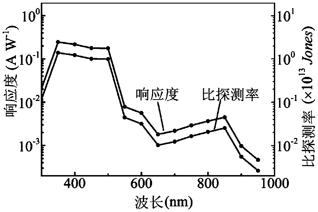
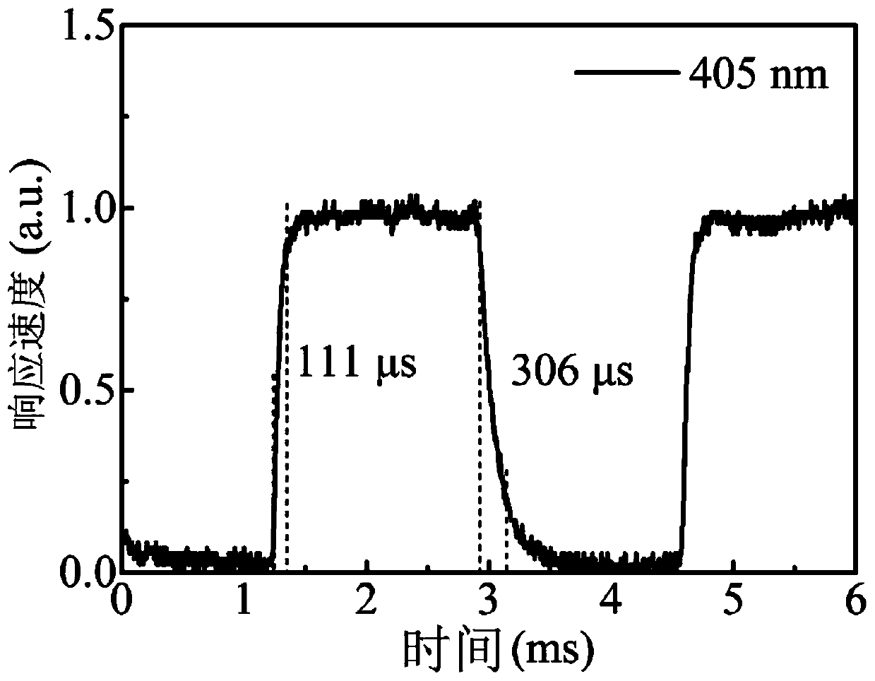
[0046] (1) Clean the ITO conductive glass ultrasonically for 20 minutes in the order of acetone, alcohol and deionized water. After drying the cleaned conductive glass, treat it with ultraviolet and ozone for 20 minutes, and use a pipette to measure 0.05mL of SnO 2 The precursor solution was spin-coated on the conductive glass, the spin-coating speed was 5000 rpm, the acceleration was 1000 rpm, and the spin-coating time was 30s. Then, place the spin-coated sample on a heating platform at 60°C for 30 minutes to form a layer of SnO on the surface of the conductive substrate. 2 film.
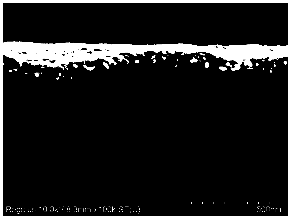
[0047] (2) Add 0.085 g of cesium bromide and 0.147 g of lead bromide into 1 mL of DMSO, stir at 70° C. for 3 hours, and react to obtain a yellow, transparent and uniform perovskite precursor solution. Use a pipette gun to measure 0.05 mL of the perovskite precursor solution and spin-coat it on the sample prepared in step (1), and then immediately use DVD-R as a template for imprinting, the imprin...
Embodiment 2
[0052] Composite photodetectors were prepared according to the method of steps (1)-(3) of Example 1, the difference being that the quality of PDPP3T and P3HT in step (3) was reduced to 1 mg and 5 mg respectively. The performance of the prepared composite photodetector is slightly lower than that in Example 1.
Embodiment 3
[0054] A composite photodetector was prepared according to the method of steps (1)-(3) of Example 1, with the difference that the embossing temperature in step (2) was lowered to 160°C. The performance of the prepared composite photodetector is slightly lower than that in Example 1.
PUM
| Property | Measurement | Unit |
|---|---|---|
| grating period | aaaaa | aaaaa |
| depth | aaaaa | aaaaa |
| width | aaaaa | aaaaa |
Abstract
Description
Claims
Application Information


