A method for preparing a pixel-level multispectral filter

A multi-spectral and optical filter technology, applied in the fields of optical filters, optics, optical components, etc., can solve the problems of poor spectral channel unit size, poor spectral passband characteristics and limitations of optical filters, etc., to improve the passband. characteristics, reducing shadow shading effects, and ensuring the effect of dimensional integrity

Active Publication Date: 2020-11-24
CHANGCHUN INST OF OPTICS FINE MECHANICS & PHYSICS CHINESE ACAD OF SCI +1
View PDF2 Cites 0 Cited by
  • Summary
  • Abstract
  • Description
  • Claims
  • Application Information

AI Technical Summary

Problems solved by technology

[0004] At present, there are roughly two preparation methods for pixel-level multispectral filters. One method is based on the Fab cavity film structure. The intermediate cavity layer is etched to form micron-scale steps of different thicknesses to adjust the spectral peak position, and finally the second reflective film stack is plated to form an array-like periodic arrangement of pixel-level multi-spectral filters. The spectral channel transmittance of the filter is low, the half-width of the channel is narrow, and the spectral range is also very limited
The other is based on a wide-band pass film structure. First, use the Lift-off photolithography process to pattern micron-scale spectral channel units on the substrate, then plate a wide-band pass film stack, and finally remove the photoresist to form a A spectral channel, repeating the above steps to form an array-type periodic arrangement of pixel-level multi-spectral filters, this method due to the shadow shielding effect during coating causes the size of the spectral channel unit to deteriorate, and the thickness of the coated broadband pass-through film stack is limited. The prepared optical filter has poor spectral passband characteristics

Method used


Image

  • A method for preparing a pixel-level multispectral filter
  • A method for preparing a pixel-level multispectral filter

Examples


preparation example Construction

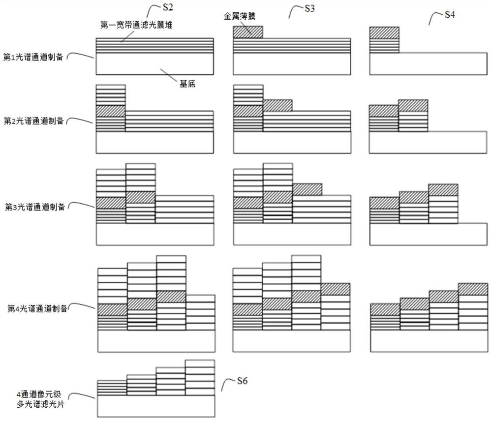
[0030] The invention provides a method for preparing a pixel-level multispectral filter, comprising the following steps:

[0031] S1: Use the film system design software to design the structure of the broadband filter film stack, the average transmittance of the designed passband is better than 85%, and the average transmittance of the stop band is less than 5%;

[0032] S2: cleaning the substrate, and plating a first broadband filter film stack on the substrate;

[0033] S3: Depositing a metal thin film on the first broadband filter film stack, and patterning the metal thin film, the patterned metal thin film is a metal thin film unit structure arranged periodically in an array, and the size of each metal thin film unit structure is 5-30 microns, one-to-one correspondence with the detector chip pixel;

[0034] S4: Using the patterned metal thin film as a mask layer, using a dry etching method to etch the first broadband filter film stack other than the metal mask layer to fo...

Embodiment 1

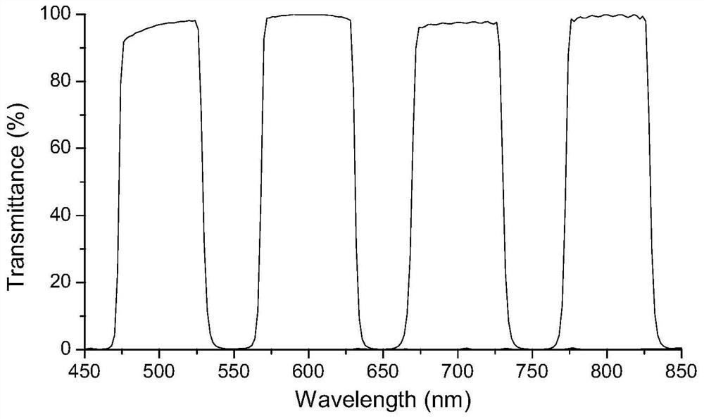
[0044] Preparation of Visible-near-infrared 4-channel pixel-level multispectral filter

[0045] Such as figure 1 As shown, it is a schematic diagram of the preparation process of the visible and near-infrared 4-channel pixel-level multispectral filter, including the following steps:

[0046] S1: Using Macleod film system design software to design a broadband filter film stack structure with a working range from 400 nm to 900 nm and a total of 4 spectral channels. The film stack structure is made of high refractive index material TiO 2 and low refractive index material SiO 2 Composed alternately, the central wavelengths of the passbands of the spectral channels are 500 nanometers, 600 nanometers, 700 nanometers, and 800 nanometers, the half-peak width of each channel is 50 nanometers, the passband transmittance is better than 95%, and the stopband average transmittance rate is less than 1%.

[0047] S2: Use ion beam-assisted electron beam evaporation coating equipment to pla...

Embodiment 2

[0054] Preparation of 6-channel short-wave infrared multi-spectral filter at pixel level

[0055] S1: Use Macleod film system design software to design a broadband filter film stack structure with a working range from 1.2 microns to 2.5 microns and a total of 6 spectral channels. The film stack structure is made of high refractive index material Si and low refractive index material Al 2 o 3 Composition, the central wavelengths of the passbands of the spectral channels are 1.4 microns, 1.6 microns, 1.8 microns, 2.0 microns, 2.2 microns, and 2.4 microns, the half-peak width of each channel is 100 nanometers, and the passband transmittance is better than 90%. The average transmittance of the stop band is less than 5%.

[0056] S2: Use the magnetron sputtering coating equipment to plate the designed first broadband filter film stack on the clean K9 glass substrate, that is, the film stack with a central wavelength of 1.4 microns. When depositing the film, the vacuum degree is 5×...


PUM

PropertyMeasurementUnit
thicknessaaaaaaaaaa
thicknessaaaaaaaaaa
wavelengthaaaaaaaaaa

Abstract

The invention provides a method for preparing a pixel-level multispectral optical filter, comprising: depositing a thicker broadband filter film stack with good spectral passband characteristics on a substrate; preparing a pattern on the bandpass filter film stack thin metal thin film; dry etching with filter film stack on the patterned metal thin film to prepare a steep stepped spectral channel unit; repeat the above steps to prepare several other spectral channel units; finally remove all spectral channels metal film on the unit. The preparation method of the pixel-level multispectral optical filter provided by the present invention can form a band-pass filter stack with a thickness of 5-15 microns thicker and periodically arranged in an array, which is conducive to improving the quality of the pixel-level multispectral optical filter. The pass-band characteristic of the spectral channel uses a patterned metal film as a mask layer and an etching stop layer to prevent the formed spectral channel unit from being etched and reduce the shadow shielding effect during the preparation process to ensure the overall size of the channel unit integrity.

Description

technical field [0001] The invention relates to the technical field of optical thin films, in particular to a method for preparing a pixel-level multispectral filter. Background technique [0002] The imaging spectrometer with spectroscopic technology as the core combines imaging technology and spectral technology. It can not only image the detection target, but also obtain its rich spectral information. Exploration, biomedical detection, security monitoring and military target early warning, identification and other fields are being widely and deeply applied. At present, imaging spectrometers often perform remote sensing work in the form of aviation, aerospace, and UAV payloads. Their volume and weight are very critical. Especially as aerospace payloads, the incompressible volume and weight greatly increase their launch costs. Therefore, there is an urgent need for the miniaturization and lightweight research of imaging spectrometers. [0003] Traditional spectroscopic me...

Claims


Application Information

Patent Timeline
Patent Type & Authority Patents(China)
IPC IPC(8): G02B5/20G02B5/28
CPCG02B5/201G02B5/285
Inventor 杨海贵张建王笑夷杨飞张卓高劲松
Owner CHANGCHUN INST OF OPTICS FINE MECHANICS & PHYSICS CHINESE ACAD OF SCI
Why Eureka
Try Eureka