Gan microwave diode with floating anode edge and its preparation method

A diode and anode technology, applied in the field of microelectronics, can solve problems such as affecting performance, and achieve the effect of improving the yield, the method is simple and effective, and the operability is strong

Active Publication Date: 2021-01-05
XIDIAN UNIV
View PDF4 Cites 0 Cited by
  • Summary
  • Abstract
  • Description
  • Claims
  • Application Information

AI Technical Summary

Problems solved by technology

However, in order to ensure the feasibility of the process, the edge of the anode needs to be placed on the AlGaN barrier layer, which will still introduce some capacitance due to the overlapping of the Schottky anode and the two-dimensional electron gas, which will affect the performance.

Method used


Image

  • Gan microwave diode with floating anode edge and its preparation method
  • Gan microwave diode with floating anode edge and its preparation method
  • Gan microwave diode with floating anode edge and its preparation method

Examples


Embodiment 1

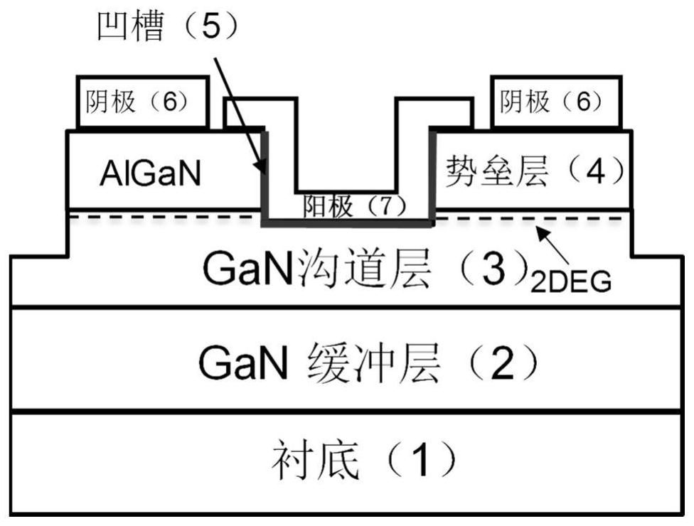
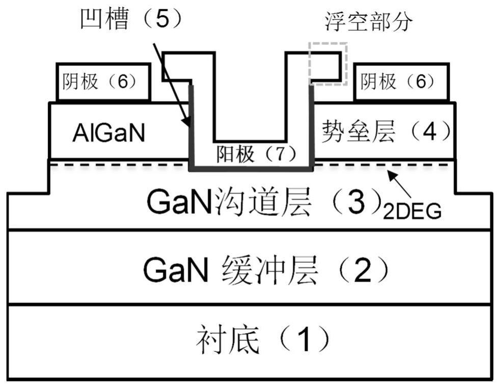
[0042] Example 1, making the anode groove etched to 5nm below the AlGaN / GaN interface, the thickness of the anode Ni / Au metal is 30 / 200nm, and the gap between the anode above the groove edge barrier layer and the lower barrier layer is 200nm. Edge floating GaN microwave diode.

[0043] Step 1, epitaxial wafer cleaning, such as Figure 4 (a).

[0044] The epitaxial wafer with a SiC substrate with a thickness of 400 μm and an AlGaN / GaN structure with a GaN buffer layer thickness of 1 μm was soaked in HF acid solution or HCl acid solution for 30 seconds, and then put into acetone solution, absolute ethanol solution and Each was ultrasonically cleaned in deionized water for 5 min, and then dried with nitrogen.

[0045] Step 2, make GaN microwave diode cathode, such as Figure 4 (b).

[0046] 2a) On a clean epitaxial wafer, perform uniform coating, baking, photolithography and development of the cathode area of ​​the device in sequence, and use electron beam evaporation equipment...

Embodiment 2

[0062] Example 2, making the anode groove etched to 10nm below the AlGaN / GaN interface, the anode Ni / Au metal thickness is 45 / 150nm, and the gap between the anode above the groove edge barrier layer and the lower barrier layer is 300nm. Edge floating GaN microwave diode.

[0063] Step 1, epitaxial wafer cleaning, such as Figure 4 (a).

[0064] The epitaxial wafer with the Si substrate with a thickness of 800 μm and the AlGaN / GaN structure with a GaN buffer layer thickness of 6 μm was soaked in HF acid solution or HCl acid solution for 30 seconds, and then put into acetone solution, absolute ethanol solution and Each was ultrasonically cleaned in deionized water for 5 min, and then dried with nitrogen.

[0065] Step 2, making GaN microwave diode cathode, such as Figure 4 (b).

[0066] The specific implementation of this step is the same as that of step 2 in Embodiment 1.

[0067] Step 3, making countertop isolation, such as Figure 4 (c).

[0068] The specific implemen...

Embodiment 3

[0078] Example 3, making the anode groove etched to 15nm below the AlGaN / GaN interface, the anode Ni / Au metal thickness is 60 / 100nm, and the gap between the anode above the groove edge barrier layer and the lower barrier layer is 100nm. Edge floating GaN microwave diode.

[0079] Step A, epitaxial wafer cleaning, such as Figure 4 (a).

[0080] Put the epitaxial wafer of AlGaN / GaN structure with a sapphire substrate with a thickness of 600 μm and an AlGaN gradient buffer layer with a thickness of 3 μm in HF acid solution or HCl acid solution for 30 seconds, then put it in acetone solution, absolute ethanol The solution and deionized water were ultrasonically cleaned for 5 min each, and then dried with nitrogen.

[0081] Step B, making GaN microwave diode cathode, such as Figure 4 (b).

[0082] The specific implementation of this step is the same as that of step 2 in Embodiment 1.

[0083] Step C, making countertop isolation, such as Figure 4 (c).

[0084] The specific...


PUM

PropertyMeasurementUnit
lengthaaaaaaaaaa
thicknessaaaaaaaaaa
thicknessaaaaaaaaaa

Abstract

The invention discloses a preparation method of a GaN microwave diode with a floating anode edge, and mainly solves the problems of large capacitance and slow frequency response of a GaN transverse microwave diode. The GaN microwave diode comprises a substrate (1), a GaN buffer layer (2), a GaN channel layer (3) and an AlGaN barrier layer (4) from bottom to top, circular grooves (5) are formed inthe channel layer and the barrier layer, and the annular cathodes (6) are arranged on the peripheral barrier layers of the grooves. The anodes (7) are arranged at the bottoms and on the side walls ofthe grooves and above the edge barrier layers of the grooves, a gap of 80-300 nm is formed between the anode above the edge barrier layer of the groove and the lower barrier layer, and a partial anodefloating structure with the length of 0.3-2 micrometers is formed. The junction capacitance of the GaN microwave diode can be greatly reduced, the frequency response of the device is remarkably improved, and the GaN microwave diode and the method can be widely applied to microwave rectification and microwave amplitude limiting.

Description

technical field [0001] The invention belongs to the technical field of microelectronics, in particular to a GaN microwave diode with an anode edge floating in the air, which can be used for microwave rectification or microwave amplitude limiting. [0002] technical background [0003] As a wide-bandgap semiconductor material, GaN material has great advantages in electrical properties. Because of its strong spontaneous polarization and piezoelectric polarization effects, the AlGaN / GaN heterojunction structure will induce High-concentration two-dimensional electron gas, because the electrons are confined in the potential well, and the impurity doping in this region is very small, so the ionized impurity scattering and alloy disorder scattering are small, the two-dimensional electron gas has extremely high mobility and electron saturation rate. Moreover, due to the inherent wide bandgap property of the material, GaN has a very large critical breakdown field strength, which is s...

Claims


Application Information

Patent Timeline
Patent Type & Authority Patents(China)
IPC IPC(8): H01L29/88H01L29/417H01L21/329
CPCH01L29/417H01L29/66219H01L29/882
Inventor 张进成党魁周弘张涛张苇杭宁静郝跃
Owner XIDIAN UNIV
Why Eureka
Try Eureka