Transmission electron microscope carrier net capable of being produced in batches and preparation method of transmission electron microscope carrier net

A technology for transmission electron microscopy and mass production, applied in circuits, discharge tubes, electrical components, etc., can solve the problems of blank and high cost, and achieve the effect of high yield, low cost and low technical level

Active Publication Date: 2020-01-31
SOUTHEAST UNIV
View PDF7 Cites 1 Cited by
  • Summary
  • Abstract
  • Description
  • Claims
  • Application Information

AI Technical Summary

Problems solved by technology

For high-mesh copper mesh, the products currently on the market mainly rely on imports, and the cost is relatively high
[0004] In addition, in the experiment of characterizing nanoparticles and nanowires with smaller size, it is generally hoped to further increase the mesh size of the mesh and reduce the mesh size, so as to realize the suspended loading of nanoparticles and nanowires, which requires a higher mesh size. , mesh shape can be designed, and the cost is relatively low. However, there is still a lack of such products in the market. At present, this technical field is still blank.

Method used


Image

  • Transmission electron microscope carrier net capable of being produced in batches and preparation method of transmission electron microscope carrier net
  • Transmission electron microscope carrier net capable of being produced in batches and preparation method of transmission electron microscope carrier net

Examples


Embodiment 1

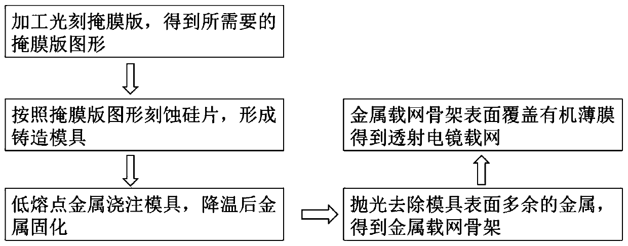
[0032] A preparation method of a mass-produced transmission electron microscope grid, the method comprising the following steps:

[0033] 1) Design and process the photolithographic mask according to the requirements of the transmission electron microscope grid, and obtain a mask pattern with a diameter of 3 mm. The mesh number in the pattern is 200 mesh, and the shape of the mesh is a square hole;

[0034] 2) transfer the mask pattern to the silicon wafer by photolithography process, and etch the mask pattern into the silicon wafer by etching process to form a casting mold, wherein the etching depth is 20 μm;

[0035] 3) Heat the casting mold to 100°C, then melt the low-melting metal bismuth-tin alloy and pour it into the mold, and the metal solidifies after cooling down to room temperature;

[0036] 4) Polishing to remove excess metal on the upper surface after the casting mold is filled, and then use adhesive tape to peel off the cast metal grid skeleton from the casting mo...

Embodiment 2

[0040] A preparation method of a mass-produced transmission electron microscope grid, the method comprising the following steps:

[0041] 1) Design and process the photolithographic mask according to the requirements of the transmission electron microscope grid, and obtain a mask pattern with a diameter of 3 mm. The mesh number in the pattern is 600 mesh, and the mesh shape is a hexagonal hole;

[0042] 2) Transfer the mask pattern to the silicon wafer by photolithography process, and etch the mask pattern into the silicon wafer by etching process to form a casting mold, wherein the etching depth is 30 μm;

[0043] 3) Heat the casting mold to 70°C, then melt the low-melting-point metal tin-indium-bismuth alloy and pour it into the mold, and the metal solidifies after cooling down to room temperature;

[0044] 4) Polishing to remove excess metal on the upper surface after the casting mold is filled, and then use adhesive tape to peel off the cast metal grid skeleton from the ca...

Embodiment 3

[0048] A preparation method of a mass-produced transmission electron microscope grid, the method comprising the following steps:

[0049] 1) Design and process the photolithographic mask according to the requirements of the transmission electron microscope grid, and obtain a mask pattern with a diameter of 3 mm. The mesh number in the pattern is 1000 mesh, and the shape of the mesh is a round hole;

[0050] 2) Transfer the mask pattern to the silicon wafer by photolithography process, and etch the mask pattern into the silicon wafer by etching process to form a casting mold, wherein the etching depth is 40 μm;

[0051] 3) Heat the casting mold to 150°C, then melt the low-melting-point metal lead-tin alloy and pour it into the mold, and the metal solidifies after cooling down to room temperature;

[0052] 4) Polishing to remove excess metal on the upper surface after the casting mold is filled, and then use adhesive tape to peel off the cast metal grid skeleton from the casting...


PUM

PropertyMeasurementUnit
thicknessaaaaaaaaaa
thicknessaaaaaaaaaa
thicknessaaaaaaaaaa

Abstract

The invention discloses a transmission electron microscope carrier net of being produced in batches and a preparation method of the transmission electron microscope carrier net. The preparation methodof the transmission electron microscope carrier net comprises the following steps that: 1) a photoetching mask is designed and processed according to the requirements of the transmission electron microscope carrier net, so that a required mask pattern is obtained; 2) the mask pattern is transferred to a silicon wafer through a photoetching process, and the mask pattern is etched into the siliconwafer through an etching process, so that a casting mold can be formed; (3) the casting mold is heated, low-melting-point metal is molten and poured into the mold, and the metal is solidified after the temperature of the metal is reduced to room temperature; (4) redundant metal on the upper surface of the casting mold filled with the metal is removed, and then a casted metal carrier net frameworkis taken out from the mold; and (5) the metal carrier net framework is covered with an organic thin-film, so that the transmission electron microscope carrier net can be formed. According to the method, on the basis of a micro-nano machining technology and the excellent characteristics of the low-melting-point metal, the electron microscope metal carrier net with 200 to 3000 meshes can be manufactured in batches. With the transmission electron microscope carrier net and the preparation method thereof of the invention adopted, a more flexible electron microscope carrier net solution can be provided for the field of electron microscope characterization.

Description

technical field [0001] The invention relates to a mass-producible transmission electron microscope grid and a preparation method thereof, belonging to the field of transmission electron microscope characterization testing. Background technique [0002] Characterizing and testing the microstructure of nanomaterials and understanding various properties of nanomaterials are important foundations for advancing the application of nanomaterials and building new functional devices. Among many testing and analysis techniques, thanks to its ultra-high resolution, transmission electron microscope analysis has become one of the most important technical methods for testing and characterizing the morphology, structure, composition and physical properties of nanomaterials. [0003] TEM grids are often an essential component in TEM test characterization. Nanomaterials that need to be tested and characterized are usually transferred to the electron microscope grid, and then the grid is ass...

Claims


Application Information

Patent Timeline
Patent Type & Authority Applications(China)
IPC IPC(8): H01J37/20H01J37/26G01N23/04G01N23/20025B22C9/06B22C9/24
CPCB22C9/061B22C9/24G01N23/04G01N23/20025H01J37/20H01J37/261
Inventor 杨宇峰贺龙兵覃天
Owner SOUTHEAST UNIV
Why Eureka
Try Eureka