

InP-based semiconductor laser structure with low contact resistance and manufacturing method thereof
A low contact resistance, semiconductor technology, used in semiconductor lasers, lasers, laser parts and other directions, can solve the problem of not involving metal-semiconductor interfaces, and achieve the effects of low contact resistance and improved heat dissipation.
- Summary
- Abstract
- Description
- Claims
- Application Information
AI Technical Summary
Problems solved by technology
Method used
Image

Examples
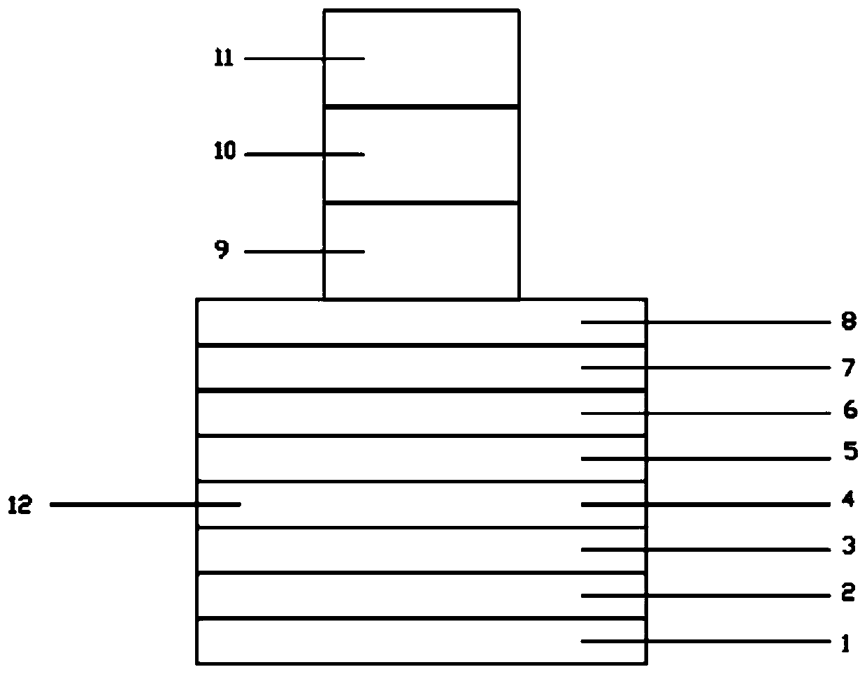
Embodiment 1
[0028] An InP-based semiconductor laser structure with low contact resistance, comprising an InP substrate 21, a semiconductor laser structure 32 epitaxially grown on the InP substrate and a metal electrode layer 31 on the semiconductor laser structure, the semiconductor laser structure comprising sequential growth from bottom to top n-InP buffer layer 22, n-type confinement layer 23, n-side waveguide layer 24, quantum well active layer 25, p-side waveguide layer 26, p-type confinement layer 27, p-type corrosion barrier layer 28, p-type cladding layer 29 and p-type electrode contact layer 30. The material of the p-type electrode contact layer 30 is p-In 0.57 Ga 0.43 As, a compressive strain of about 2600ppm is introduced into the electrode contact layer, the band gap is reduced from 0.75eV in the conventional structure to about 0.71eV, the material thickness range is 150nm, and the doping concentration level is 0.3×10 20 cm -1 .
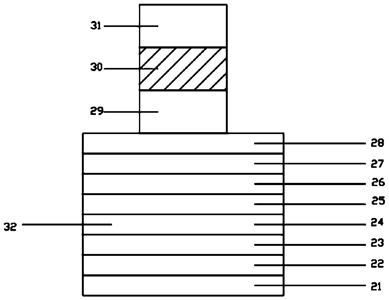
Embodiment 2
[0029] Embodiment 2, a kind of InP base semiconductor laser structure with low contact resistance, comprises InP substrate 41, the semiconductor laser structure 52 of epitaxial growth on the InP substrate and the metal electrode layer 51 on the semiconductor laser structure, the semiconductor laser structure comprises The n-InP buffer layer 42, n-type confinement layer 43, n-side waveguide layer 44, quantum well active layer 45, p-side waveguide layer 46, p-type confinement layer 47, p-type corrosion barrier layer 48, p-type cladding layer 49 and p-type electrode contact layer 50 . The material of the p-type electrode contact layer 50 is p-In 0.53+x Ga 0.47-xThe ternary or binary compound material of As, in which x gradually and continuously linearly changes from 0 to 0.47, the thickness of the material is 250 nm, and the linear relationship between x and thickness changes is x≈0.02×t (where t is the thickness, in nm), The doping concentration level is 0.3×10 20 cm -1 abou...
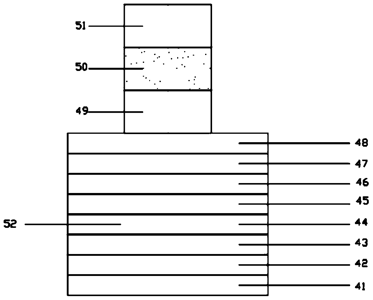
Embodiment 3
[0031] An InP-based semiconductor laser structure with low contact resistance, comprising an InP substrate 41, a semiconductor laser structure 52 epitaxially grown on the InP substrate and a metal electrode layer 51 on the semiconductor laser structure, the semiconductor laser structure comprising sequential growth from bottom to top n-InP buffer layer 42, n-type confinement layer 43, n-side waveguide layer 44, quantum well active layer 45, p-side waveguide layer 46, p-type confinement layer 47, p-type corrosion barrier layer 48, p-type cladding layer 49 and the p-type electrode contact layer 50, the p-type electrode contact layer, the material is a ternary or binary compound material of p-In0.53+xGa0.47-xAs, wherein x gradually and continuously changes from 0 to 0.47, and the thickness of the material is At 250 nm, the parabolic relationship of x varying with thickness is x≈1E-05×t 2 -0.0024t (where t is the thickness in nm), the doping concentration level is 0.3×10 20 cm -...
PUM
| Property | Measurement | Unit |
|---|---|---|
| Thickness | aaaaa | aaaaa |
| Thickness | aaaaa | aaaaa |
| Thickness | aaaaa | aaaaa |
Abstract
Description
Claims
Application Information