GaN/AlGaN heterojunction material based on monocrystalline diamond substrate and preparation method of GaN/AlGaN heterojunction material
A single crystal diamond and heterojunction technology, applied in the field of microelectronics, can solve the problems of large lattice mismatch between GaN and diamond, difficult growth of diamond substrates, limiting device characteristics, etc., and achieves low cost, reduced stress, and simplified The effect of craft difficulty
- Summary
- Abstract
- Description
- Claims
- Application Information
AI Technical Summary
Problems solved by technology
Method used
Image

Examples
Embodiment 1
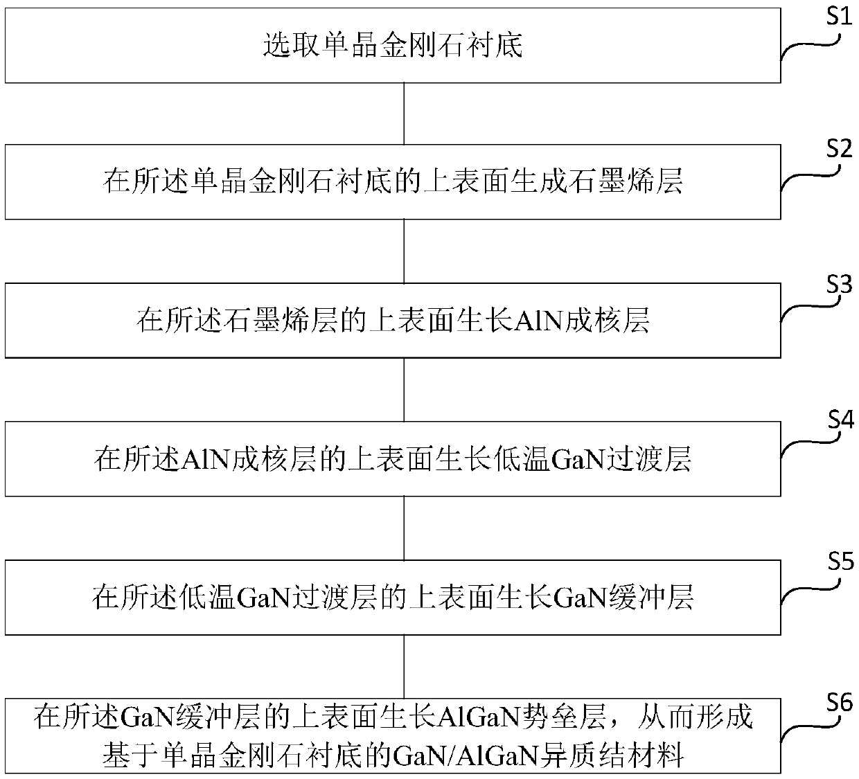
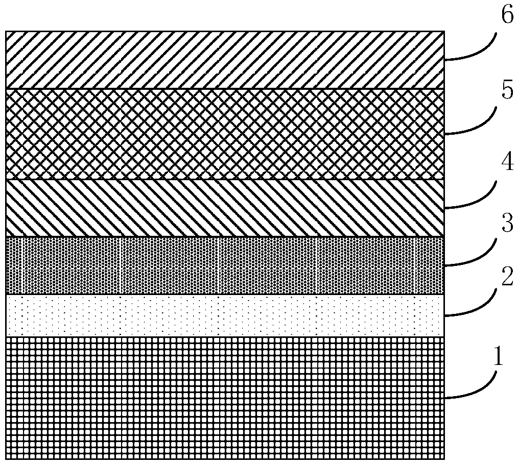
[0042] See figure 1 , figure 1 It is a flowchart of a method for preparing a GaN / AlGaN heterojunction material based on a single crystal diamond substrate provided by an embodiment of the present invention. The preparation method of the present embodiment comprises:
[0043] S1: Select a single crystal diamond substrate;
[0044] S2: generating a graphene layer on the upper surface of the single crystal diamond substrate;
[0045] S3: growing an AlN nucleation layer on the upper surface of the graphene layer;
[0046] S4: growing a low-temperature GaN transition layer on the upper surface of the AlN nucleation layer;
[0047] S5: growing a GaN buffer layer on the upper surface of the low-temperature GaN transition layer;
[0048] S6: growing an AlGaN barrier layer on the upper surface of the GaN buffer layer to finally form a GaN / AlGaN heterojunction material based on a single crystal diamond substrate.
[0049] Further, the S1 includes:
[0050] A single crystal diamon...
Embodiment 2
[0070] On the basis of the above examples, to prepare a GaN / AlGaN heterogeneous diamond substrate based on (100) crystal plane single crystal diamond substrate and including 20nm AlN nucleation layer, 20nm low temperature GaN transition layer, 0.1μm GaN buffer layer and 10nm AlGaN barrier layer Taking the textured material as an example, this embodiment describes the preparation method of the embodiment of the present invention in detail.
[0071] The preparation method of the present embodiment comprises:
[0072] Step 1: Select a single crystal diamond substrate;
[0073] A single crystal diamond with a thickness of 0.5 mm and a crystal plane of (100) was selected as the substrate.
[0074] Step 2: generate a graphene layer on the upper surface of the (100) single crystal diamond substrate;
[0075] Specifically, a graphene layer of 0.2 mm is grown on a metal substrate by chemical vapor deposition; 18 hours in the mixed solution of 2 mixing, remove metal substrate; Finall...
Embodiment 3
[0087] In this example, by preparing a GaN / AlGaN heterogeneous substrate based on (110) crystal plane single crystal diamond substrate, including 100nm AlN nucleation layer, 200nm low temperature GaN transition layer, 0.5μm GaN buffer layer and 100nm AlGaN barrier layer Taking the junction material as an example, the preparation method of the embodiment of the present invention is described in detail.
[0088] The preparation method of the present embodiment comprises:
[0089] Step 1: Select a single crystal diamond substrate;
[0090] A single crystal diamond with a thickness of 0.5 mm and a crystal plane of (110) was selected as the substrate.
[0091] Step 2: generate a graphene layer on the upper surface of the (110) single crystal diamond substrate;
[0092] Specifically, adopt chemical vapor deposition method to grow 0.3mm graphene layer on metal substrate; Then the metal substrate covered with graphene layer is placed in 1mol / L ferric chloride and 2mol / L hydrochloric...
PUM
| Property | Measurement | Unit |
|---|---|---|
| Thickness | aaaaa | aaaaa |
| Thickness | aaaaa | aaaaa |
| Thickness | aaaaa | aaaaa |
Abstract
Description
Claims
Application Information
 - R&D
- Intellectual Property
- Life Sciences
- Materials
- Tech Scout
- Unparalleled Data Quality
- Higher Quality Content
- 60% Fewer Hallucinations
Browse by: Latest US Patents, China's latest patents, Technical Efficacy Thesaurus, Application Domain, Technology Topic, Popular Technical Reports.
© 2025 PatSnap. All rights reserved.Legal|Privacy policy|Modern Slavery Act Transparency Statement|Sitemap|About US| Contact US: help@patsnap.com