Perovskite LED device based on surface ligand control and preparation method thereof

A light-emitting diode and perovskite technology, which is applied in the field of perovskite light-emitting diode devices and their preparation, can solve problems such as research on the electroluminescent properties of light-emitting diode devices, and achieve the goals of reducing leakage current, high repeatability, and suppressing the formation of defects Effect

Inactive Publication Date: 2020-03-06
SUZHOU UNIV
View PDF7 Cites 17 Cited by
  • Summary
  • Abstract
  • Description
  • Claims
  • Application Information

AI Technical Summary

Problems solved by technology

CN201910180380.4 discloses a two-dimensional perovskite material. The two-dimensional perovskite material is composed of regular octahedral inorganic anions composed of organic cations containing hydrophobic amine groups and lead halide. Prevent water vapor from penetrating into the inorganic regular octahedron, thereby preventing perovskite from hydrolysis and enhancing the stability of perovskite in a humid environment, but it does not affect the electroluminescence performance of light-emitting diode devices formed using this two-dimensional perovskite material. research, which shows that its luminous performance needs to be further improved

Method used


Image

  • Perovskite LED device based on surface ligand control and preparation method thereof
  • Perovskite LED device based on surface ligand control and preparation method thereof
  • Perovskite LED device based on surface ligand control and preparation method thereof

Examples


Embodiment 1

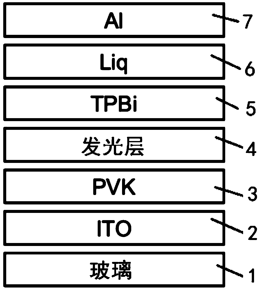
[0043] Such as figure 1 As shown, a perovskite light-emitting diode device based on surface ligand control of the present invention includes glass 1, ITO2, PVK layer 3, light-emitting layer 4, TPBi layer 5, Liq layer 6, Al electrode layer 7. Its preparation method steps are as follows:

[0044] Step 1: Use a nano-sponge dipped in cleaning agent to scrub the ITO glass and rinse it with deionized water. Place it in a beaker and put it in an ultrasonic water bath. Use ethanol, acetone and deionized water to ultrasonically clean it for 15 minutes and repeat 2-3 times. After cleaning, put the beaker containing the ITO glass in a drying oven to heat and dry it, and finally put the ITO glass face up in a watch glass, and treat it in a UV-ozone cleaning machine for 15 minutes;

[0045] Step 2: Filter the poly(9-vinylcarbazole) solution through a 0.22 μm filter head, and spin it on the ITO glass at a rotation speed of 3500-4500 rpm for 40-60 seconds, and then anneal at 100-110 ° C fo...

Embodiment 2

[0050] A preparation method of a perovskite light-emitting diode device based on surface ligand control, the preparation steps of the preparation method are as follows:

[0051] Step 1: Use a nano-sponge dipped in cleaning agent to scrub the ITO glass and rinse it with deionized water. Place it in a beaker and put it in an ultrasonic water bath. Use ethanol, acetone and deionized water to ultrasonically clean it for 15 minutes and repeat 2-3 times. After cleaning, put the beaker containing the ITO glass in a drying oven to heat and dry it, and finally put the ITO glass face up in a watch glass, and treat it in a UV-ozone cleaning machine for 15 minutes;

[0052] Step 2: Filter the poly(9-vinylcarbazole) solution through a 0.22 μm filter head, and spin it on the ITO glass at a speed of 3500-4500 rpm for 40-60 seconds, and then anneal at 100-110 ° C for 10-15 minutes;

[0053] Step 3: The precursor materials of cesium bromide, lead bromide and phenethylammonium bromide are disso...

Embodiment 3

[0057] A preparation method of a perovskite light-emitting diode device based on surface ligand control, the preparation steps of the preparation method are as follows:

[0058] Step 1: Use a nano-sponge dipped in cleaning agent to scrub the ITO glass and rinse it with deionized water. Place it in a beaker and put it in an ultrasonic water bath. Use ethanol, acetone and deionized water to ultrasonically clean it for 15 minutes and repeat 2-3 times. After cleaning, put the beaker containing the ITO glass in a drying oven to heat and dry it, and finally put the ITO glass face up in a watch glass, and treat it in a UV-ozone cleaning machine for 15 minutes;

[0059] Step 2: Filter the poly(9-vinylcarbazole) solution through a 0.22 μm filter head, and spin it on the ITO glass at a rotation speed of 3500-4500 rpm for 40-60 seconds, and then anneal at 100-110 ° C for 10-15 minutes;

[0060] Step 3: The precursor materials of cesium bromide, lead bromide and phenethylammonium bromide ...


PUM


Abstract

The invention relates to a method for preparing a perovskite LED device based on surface ligand control, including the following steps: applying an organic solution of a hole injection layer materialto the surface of a conductive substrate, and forming a hole injection layer after annealing; dissolving cesium bromide, lead bromide and phenethylamine bromide in an organic solvent under the effectof a 3-(decyl dimethyl ammonium) propane-1-sulfonic acid inner salt surfactant to obtain a perovskite precursor solution, applying the perovskite precursor solution to the surface of the hole injection layer and obtaining a perovskite film after annealing; treating the surface of the perovskite film with an alkylamine organic solution to form a light-emitting layer; and successively preparing an electron transport layer, an electron injection layer and a metal cathode electrode on the surface of the light-emitting layer. The method of the invention is simple and convenient, has a wide range ofmaterials and good repeatability, and can achieve the device performance. Through surface ligand exchange, the flatness and uniformity of the perovskite film are improved, the formation of defects iseffectively suppressed, and the overall performance of the device is significantly improved.

Description

technical field [0001] The invention relates to the field of semiconductor devices, in particular to a perovskite light-emitting diode device based on surface ligand control and a preparation method thereof. Background technique [0002] Perovskite material has unique photoelectric characteristics, its low exciton binding energy (50-37meV), high carrier mobility, and high absorption coefficient make it have a good performance in the field of light-emitting diodes. The perovskite structure can Without high-temperature treatment, polycrystalline thin films are constructed by a simple solution process, which has high application potential on large-area flexible light-emitting substrates, due to their strong photoluminescence properties and adjustable band gap of polycrystalline materials full width at half maximum (FWHM), making them highly potential for use in light-emitting diodes. Therefore, the application research of perovskite in the field of light-emitting diodes has be...

Claims


Application Information

Patent Timeline
Patent Type & Authority Applications(China)
IPC IPC(8): H01L51/56H01L51/50H01L51/54
CPCH10K71/12H10K71/40H10K85/60H10K50/11H10K71/00
Inventor 廖良生沈万姗苑帅田起生
Owner SUZHOU UNIV
Why Eureka
Try Eureka