Glass-sealed voltage regulation diode, tube core and manufacturing method thereof

A voltage adjustment, diode technology, applied in semiconductor/solid-state device manufacturing, circuits, electrical components, etc., can solve problems such as the difference in thermal expansion coefficient between the die and the glass shell, device cracking, breakdown leakage, etc., to reduce leakage current, The effect of avoiding stress difference and eliminating parasitic capacitance

Pending Publication Date: 2020-03-24
BEIJING MXTRONICS CORP +1
View PDF9 Cites 3 Cited by
  • Summary
  • Abstract
  • Description
  • Claims
  • Application Information

AI Technical Summary

Problems solved by technology

The traditional voltage adjustment diode is not protected by a composite passivation layer, and it is prone to breakdown and leakage in a high-current environment, causing damage to the device; and there is a difference in thermal expansion coefficient between the die and the glass shell, which will also cause the packaged device to be damaged in harsh environments. failure due to lower cracking

Method used


Image

  • Glass-sealed voltage regulation diode, tube core and manufacturing method thereof
  • Glass-sealed voltage regulation diode, tube core and manufacturing method thereof
  • Glass-sealed voltage regulation diode, tube core and manufacturing method thereof

Examples


preparation example Construction

[0043] The preparation method of the above-mentioned voltage adjustment diode die includes the following steps:

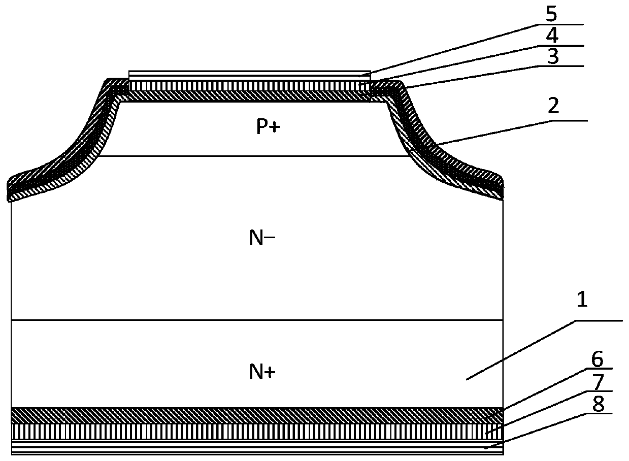
[0044] s1-1. Diffusion and deep junction diffusion of the silicon wafer 1 are carried out sequentially to form a PN junction with a certain junction depth on the front side of the silicon wafer 1; the silicon wafer 1 can be an N-type silicon wafer, using N type, The thickness is 220 μm, and a PN junction is formed through a diffusion process, and a deep junction diffusion process is performed on the PN junction to form a PN junction with a junction depth of 18-22um; of course, the silicon wafer 1 can also be a P-type silicon wafer.

[0045] (s1-2), performing wet etching treatment on the periphery of the front surface of the silicon wafer 1 to generate an arc-shaped gap to form a central island area for attaching the first electrode;

[0046] (s1-3), performing passivation treatment on the front side of the silicon wafer, depositing the first silicon dioxide layer,...

Embodiment 1

[0061] In this embodiment, a glass-encapsulated voltage-adjusting diode die is prepared, which includes the following steps:

[0062] s1-1. Diffusion and deep junction diffusion of the silicon wafer 1 are carried out sequentially to form a PN junction with a certain junction depth on the front side of the silicon wafer 1; the silicon wafer 1 can be an N-type silicon wafer, using N type, The thickness is 220 μm, and a PN junction is formed through a diffusion process, and a deep junction diffusion process is performed on the PN junction to form a PN junction with a junction depth of 18 um; of course, the silicon wafer 1 can also be a P-type silicon wafer.

[0063] (s1-2), performing wet etching treatment on the periphery of the front surface of the silicon wafer 1 to generate an arc-shaped gap to form a central island area for attaching the first electrode;

[0064] (s1-3), carry out passivation treatment to the front side of the silicon wafer, deposit the first silicon dioxide...

Embodiment 2

[0076] In this embodiment, a glass-encapsulated voltage-adjusting diode die is prepared, which includes the following steps:

[0077] s1-1. Diffusion and deep junction diffusion of the silicon wafer 1 are carried out sequentially to form a PN junction with a certain junction depth on the front side of the silicon wafer 1; the silicon wafer 1 can be a P-type silicon wafer, using a P type, The thickness is 525 μm, and a PN junction is formed through a diffusion process, and a deep junction diffusion process is performed on the PN junction to form a PN junction with a junction depth of 22 μm; of course, the silicon wafer 1 can also be an N-type silicon wafer.

[0078] (s1-2), performing wet etching treatment on the periphery of the front surface of the silicon wafer 1 to generate an arc-shaped gap to form a central island area for attaching the first electrode;

[0079] (s1-3), carry out passivation treatment to the front side of the silicon wafer, deposit the first silicon dioxi...


PUM

PropertyMeasurementUnit
thicknessaaaaaaaaaa
thicknessaaaaaaaaaa

Abstract

The invention relates to a glass-sealed voltage regulation diode, a tube core and a manufacturing method thereof. The tube core comprises a silicon wafer, a passivation protection layer, a first electrode and a second electrode. Arc-shaped gaps are formed around the front surface of the silicon wafer; an island area is formed in the center, a first electrode is attached to the center island area on the front face of a silicon wafer, a second electrode is attached to the back face of the silicon wafer, a passivation protection layer avoids the first electrode and is attached to an arc notch ofthe silicon wafer, and the passivation protection layer is of a three-layer composite structure and sequentially comprises a first silicon dioxide layer, a PSG layer and a second silicon dioxide layerfrom the silicon wafer to the outside. The diode further comprises a first tungsten column, a second tungsten column, a glass outer cover, a first lead end and a second lead end on the basis of the tube core, the first tungsten column and the second tungsten column are respectively welded with the first electrode and the second electrode, and the first lead end and the first lead end are respectively welded with the first tungsten column and the second tungsten column; the glass outer cover is packaged on the outer sides of the first tungsten column and the second tungsten column and used forprotecting the tube core. The diode is low in thermal resistance and high in reliability.

Description

technical field [0001] The invention relates to a glass-encapsulated voltage adjusting diode and a manufacturing method thereof, which belong to the field of semiconductor devices. Background technique [0002] Due to the characteristics of stable voltage, high precision, low leakage current, high reliability, and long life, the voltage adjustment diode can effectively adjust the voltage in the circuit and solve the problem of breakdown caused by excessive voltage. Voltage adjustment diodes are mainly used in switching power supplies, frequency converters, drivers and other circuits. They are one of the most important electronic components in electronic circuits. They have been widely used in various civil and military electronic fields, especially in aerospace, aviation and weapons. In the application of equipment and other fields, the requirements for its reliability are becoming higher and higher. [0003] In addition to high accuracy of voltage adjustment, parasitic cap...

Claims


Application Information

Patent Timeline
Patent Type & Authority Applications(China)
IPC IPC(8): H01L29/861H01L23/31H01L23/29H01L29/45H01L29/06H01L21/56H01L21/28H01L21/329H01L21/60
CPCH01L23/291H01L23/3171H01L29/45H01L29/8613H01L29/0657H01L29/6603H01L21/56H01L21/28H01L24/81H01L2224/33181
Inventor 刘学明王华赵昕张文敏
Owner BEIJING MXTRONICS CORP
Why Eureka
Try Eureka