Method and equipment for batch production of AR diffracted optical waveguides
A diffracted light, batch technology, applied in the direction of optical waveguide light guide, opto-mechanical equipment, light guide, etc., can solve the problems of small imprinting area, easily damaged mold, many demoulding defects, etc., to reduce the imprinting force, The effect of high production efficiency, improved imprint accuracy and quality
- Summary
- Abstract
- Description
- Claims
- Application Information
AI Technical Summary
Problems solved by technology
Method used
Image
Examples
Embodiment 1
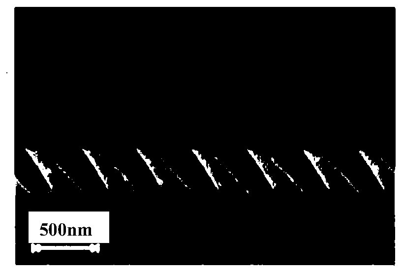
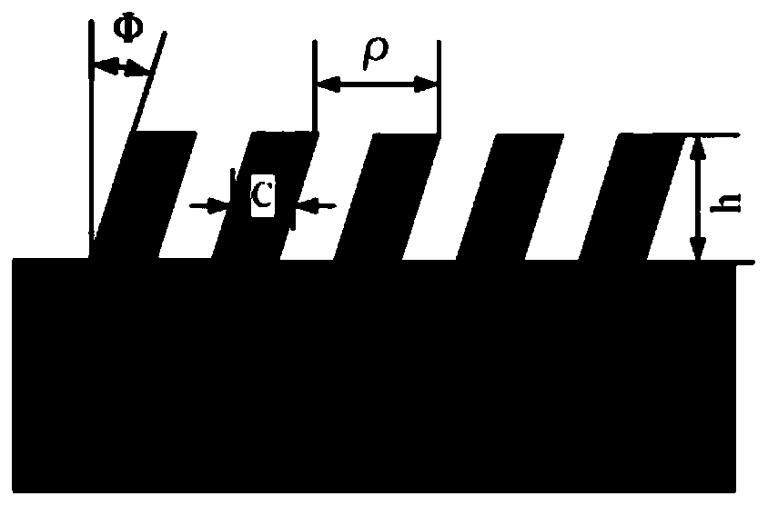
[0073] Figure 1(a) and Figure 1(b) are schematic diagrams of a diffractive optical waveguide (surface relief tilted grating) to be fabricated. The inclination angle, groove depth (relative depth), and fill factor (grating width / period) are as shown in the figure. The parameters of the surface relief oblique grating to be manufactured in this implementation example: inclination angle 30 ° ; groove depth 600nm; fill factor (coefficient) 50%.
[0074] For surface relief tilted grating diffraction optical waveguide, tilted grating nanostructures, especially tilted grating with large tilt angle, large groove depth and large area surface relief tilted grating with arbitrary shape, various existing micro-nano fabrication techniques, such as electron beam lithography , nanoimprinting, optical lithography, interference lithography, laser processing, etc. cannot be manufactured. Because the existing micro-nano manufacturing technologies are all based on planar micro-nano patterning (t...
Embodiment 2
[0124] The difference from the first embodiment is that the process parameters of each step can be changed. at the same time,
[0125] After the first production cycle is completed, process steps 1, 2 and 3 are run in parallel with process steps 4 and 5.
Embodiment 3
[0127] The difference from the first embodiment is that the process parameters of each step can be changed. At the same time, process step 1, step 2 and step 3 are implemented serially in advance.
[0128] The actual process steps only include step 4 and step 5, and run in sequence.
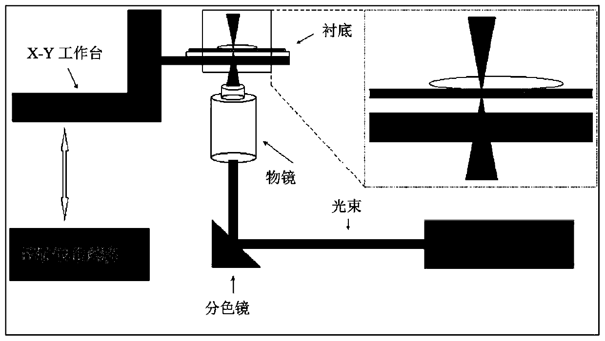
[0129] The equipment used in the above embodiments mainly includes: two-photon polymerization micro-nano 3D printer; precision micro-electroforming equipment; working soft mold replication equipment; composite nanoimprint lithography equipment;
PUM
| Property | Measurement | Unit |
|---|---|---|
| thickness | aaaaa | aaaaa |
| thickness | aaaaa | aaaaa |
| thickness | aaaaa | aaaaa |
Abstract
Description
Claims
Application Information


