LED epitaxial structure growth method

A growth method and epitaxial structure technology, which can be used in coatings, gaseous chemical plating, semiconductor devices, etc., can solve the problems of low quantum well radiation recombination efficiency and low quantum well growth quality, etc. The effect of increasing hole mobility and luminous radiation efficiency

Active Publication Date: 2020-04-03
XIANGNENG HUALEI OPTOELECTRONICS
View PDF26 Cites 4 Cited by
  • Summary
  • Abstract
  • Description
  • Claims
  • Application Information

AI Technical Summary

Problems solved by technology

[0005] The invention solves the problems of low quantum well growth quality and low quantum well radiation recombination efficiency existing in the existing LED epitaxial growth method by adopting a new multi-quantum well layer growth method, thereby improving the luminous efficiency of the LED and reducing the forward driving voltage

Method used


Image

  • LED epitaxial structure growth method
  • LED epitaxial structure growth method
  • LED epitaxial structure growth method

Examples


Embodiment 1

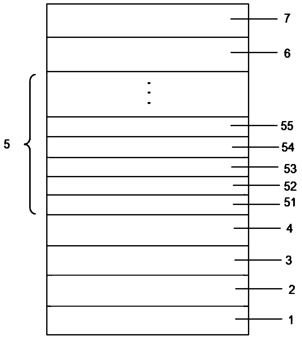
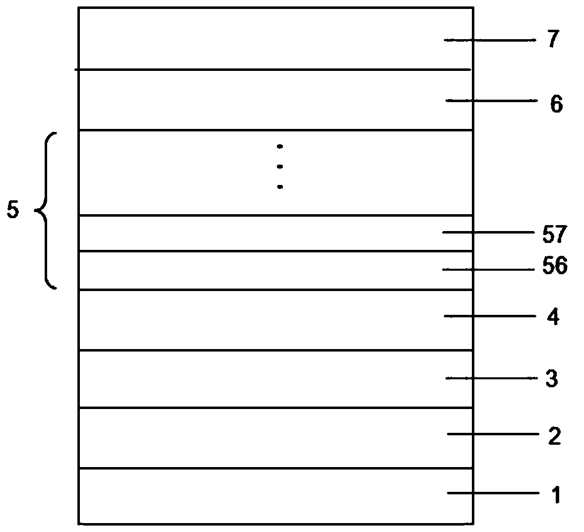
[0041] This embodiment adopts the LED epitaxial structure growth method provided by the present invention, adopts MOCVD to grow high-brightness GaN-based LED epitaxial wafers, and uses high-purity H 2 or high purity N 2 or high purity H 2 and high purity N 2 The mixed gas as the carrier gas, high-purity NH 3 As the N source, the metal-organic source trimethylgallium (TMGa) is used as the gallium source, trimethylindium (TMIn) is used as the indium source, and the N-type dopant is silane (SiH 4 ), trimethylaluminum (TMAl) as the aluminum source, and the P-type dopant as magnesium dicene (CP 2 Mg), the reaction pressure is between 70mbar and 900mbar. The specific growth method is as follows (for the epitaxial structure, please refer to figure 1 ):

[0042] A method for growing an LED epitaxial structure, which sequentially includes: processing a substrate 1, growing a low-temperature buffer layer GaN2, growing an undoped GaN layer 3, growing a Si-doped N-type GaN layer 4, ...


PUM

PropertyMeasurementUnit
thicknessaaaaaaaaaa
thicknessaaaaaaaaaa
thicknessaaaaaaaaaa

Abstract

The invention discloses an LED epitaxial structure growth method. The method comprises the following steps: processing a substrate, growing a low-temperature buffer layer GaN, growing an undoped GaN layer, growing a Si-doped N-type GaN layer, growing a multi-quantum well layer, growing an AlGaN electronic barrier layer, and growing a Mg-doped P-type GaN layer, and performing cooling, wherein the growth of the multi-quantum well layer sequentially comprises the steps of growing an N2 gradient atmosphere InxGa(1-x)N-1 layer, growing an H2 gradient atmosphere InxGa(1-x)N-2 layer, growing an H2 and N2 mixed atmosphere InxGa(1-x)N-3 layer, growing a GaN layer and growing a GaN layer. According to the method, the problems of low quantum well growth quality and low quantum well radiation recombination efficiency in the existing LED epitaxial growth method are solved, so that the luminous efficiency of the LED is improved, and the forward driving voltage is reduced.

Description

technical field [0001] The invention belongs to the technical field of LEDs, and in particular relates to a method for growing an LED epitaxial structure. Background technique [0002] A light-emitting diode (Light-Emitting Diode, LED) is a semiconductor electronic device that converts electrical energy into light energy. When current flows, electrons and holes recombine in their quantum wells to emit monochromatic light. As a high-efficiency, environmentally friendly, and green new solid-state lighting source, LED has the advantages of low voltage, low power consumption, small size, light weight, long life, high reliability, and rich colors. At present, the scale of domestic production of LEDs is gradually expanding, but LEDs still have the problem of low luminous efficiency, which affects the energy-saving effect of LEDs. [0003] In the current traditional LED epitaxy InGaN / GaN multi-quantum well layer growth method, the quality of the InGaN / GaN multi-quantum well layer...

Claims


Application Information

Patent Timeline
Patent Type & Authority Applications(China)
IPC IPC(8): H01L33/06H01L33/00C23C16/34C23C16/52
CPCH01L33/06H01L33/007C23C16/34C23C16/52
Inventor 徐平苗振林季辉唐海马谢鹏杰
Owner XIANGNENG HUALEI OPTOELECTRONICS
Why Eureka
Try Eureka