Preparation method of visible-short wave infrared light detection substrate based on oxide/gold nanorod/silicon
A technology of gold nanorods and infrared light, which is applied in the direction of climate sustainability, final product manufacturing, sustainable manufacturing/processing, etc., can solve the problems of high carrier recombination rate, limited light absorption intensity, and hindering the application of silicon. Achieve the effects of wide spectral response range, maintaining stability, and good detection characteristics
- Summary
- Abstract
- Description
- Claims
- Application Information
AI Technical Summary
Problems solved by technology
Method used
Image

Examples
Embodiment 1
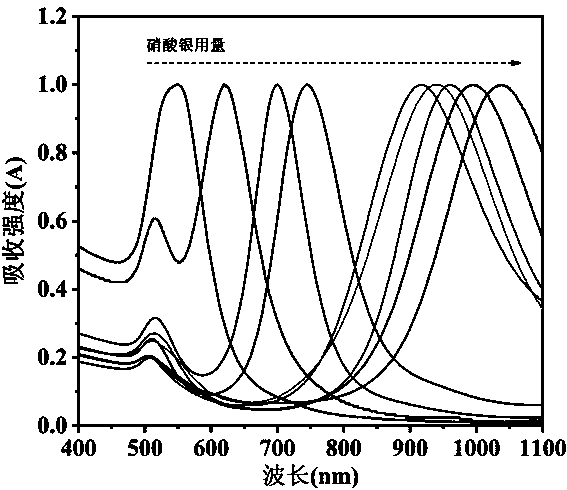
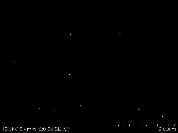
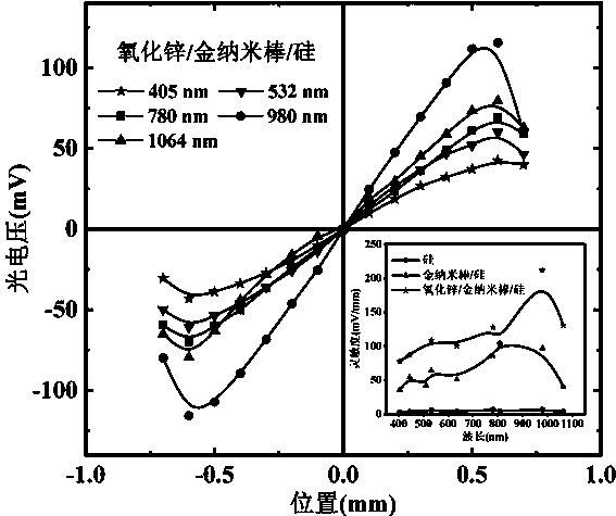
[0025] A visible-shortwave infrared photodetection substrate based on oxide / gold nanorods / silicon, which synthesizes small-sized gold nanorods with different aspect ratios by a silver-induced seedless method; The absorbing layer is annealed to obtain a more tightly bonded gold nanorod / silicon wafer substrate; different oxide films are deposited on the surface of the gold nanorod / silicon wafer substrate to form a heterojunction structure with good photoelectric response, and finally the oxide / gold nanorods / silicon substrate Novel visible-short-wave infrared light detection substrate, prepared according to the following steps:
[0026] (1) Synthesis of gold nanorods with different aspect ratios: using silver-induced seedless method, using 0.22 M CTAB solution as the growth solution, adding 9.12 ml 10 mM HAuCl to 192.49 ml 0.22 M CTAB solution in sequence 4 solution, 5.4 ml10 mM AgNO 3 solution and 22.8 ml 0.053 M hydroquinone solution, after the solution became colorless, add ...
Embodiment 2
[0033] A visible-short-wave infrared light detection substrate based on oxide / gold nanorod / silicon, similar to Example 1, prepared according to the following steps:
[0034] (1) Synthesis of gold nanorods with different aspect ratios: using silver-induced seedless method, using 0.22 M CTAB solution as the growth solution, adding 9.12 ml 10 mM HAuCl to 192.49 ml 0.22 M CTAB solution in sequence 4 solution, 0.9 ml 10 mM AgNO 3 solution, 22.8 ml 0.053 M hydroquinone solution, after the solution became colorless, add 18 μl 17.05 mM NaBH to the solution at a stirring rate of 1500 rpm 4 The ice-water mixture solution (0°C), stirring the solution for 2 minutes, then standing at a constant temperature of 30°C for more than 12 hours to fully react, centrifuged the above solution three times at 11,000 rpm for 15 minutes to remove CTAB in the solution, and obtained longitudinal surface plasmons Gold nanorods with excitonic absorption peak at 600nm;
[0035] (2) Load gold nanorods onto ...
Embodiment 3
[0039] A visible-short-wave infrared light detection substrate based on oxide / gold nanorod / silicon, similar to Example 1, prepared according to the following steps:
[0040] (1) Synthesis of gold nanorods with different aspect ratios: using silver-induced seedless method, using 0.22 M CTAB solution as the growth solution, adding 9.12 ml 10 mM HAuCl to 192.49 ml 0.22 M CTAB solution in sequence 4 solution, 3.6 ml10 mM AgNO 3 solution, 22.8 ml 0.053 M hydroquinone solution, after the solution became colorless, add 27.6 μl 17.05 mM NaBH to the solution at a stirring rate of 1000 rpm 4 The ice-water mixture solution (0°C), kept stirring for 2 minutes, then kept the solution at a constant temperature of 30°C for more than 12 hours, centrifuged the above solution three times at 11,000 rpm for 15 minutes to remove CTAB in the solution, and obtained longitudinal surface plasmons Gold nanorods with excitonic absorption peak at 850nm;
[0041] (2) Au nanorods loaded on the surface of ...
PUM
 Abstract
Description
Claims
Application Information
 - Generate Ideas
- Intellectual Property
- Life Sciences
- Materials
- Tech Scout
- Unparalleled Data Quality
- Higher Quality Content
- 60% Fewer Hallucinations
Browse by: Latest US Patents, China's latest patents, Technical Efficacy Thesaurus, Application Domain, Technology Topic, Popular Technical Reports.
© 2025 PatSnap. All rights reserved.Legal|Privacy policy|Modern Slavery Act Transparency Statement|Sitemap|About US| Contact US: help@patsnap.com