Manufacturing method of SiC power device chip gate oxide layer and power device

A manufacturing method and technology for power devices, applied in the fields of semiconductor/solid-state device manufacturing, semiconductor devices, electrical components, etc., can solve problems affecting device reliability, reducing interface state density, reducing interface state density, etc., and improving gate reliability. performance, eliminate defects, and reduce device manufacturing costs

Active Publication Date: 2020-04-14
SOUTH UNIVERSITY OF SCIENCE AND TECHNOLOGY OF CHINA
View PDF8 Cites 3 Cited by
  • Summary
  • Abstract
  • Description
  • Claims
  • Application Information

AI Technical Summary

Problems solved by technology

[0005]1. Directly grow a low-defect SiC / SiO2 interface on SiC single crystal or epitaxial wafer: the method is through low temperature and low oxygen content Annealing and high temperature thermal oxidation grow SiC / SiO2 interface, this method can improve gate reliability, but the effect of reducing the interface state density is not obvious
[0006]2. Introducing other elements into the SiC / SiO2 interface region to form traps: Traps can reduce the interface state density, but the introduction of additional elements has potential will have some negative impact on the device
For example, excessive P passivation will combine with SiO2 to form phosphosilicate glass (PSG), this unstable substance will seriously affect the integrity of the gate oxide layer, resulting in increased gate leakage current , affecting the reliability of the long-term work of the device

Method used


Image

  • Manufacturing method of SiC power device chip gate oxide layer and power device
  • Manufacturing method of SiC power device chip gate oxide layer and power device
  • Manufacturing method of SiC power device chip gate oxide layer and power device

Examples


Embodiment Construction

[0031] The subject matter of the invention will now be discussed with reference to several exemplary embodiments. It should be understood that these embodiments are discussed only to enable those of ordinary skill in the art to better understand and thus implement the content of the present invention, and do not imply any limitation on the scope of the present invention.

[0032] As used herein, the term "comprising" and variations thereof are to be read as open-ended terms meaning "including but not limited to". The term "based on" is to be read as "based at least in part on". The terms "one embodiment" and "an embodiment" are to be read as "at least one embodiment." The term "another embodiment" is to be read as "at least one other embodiment".

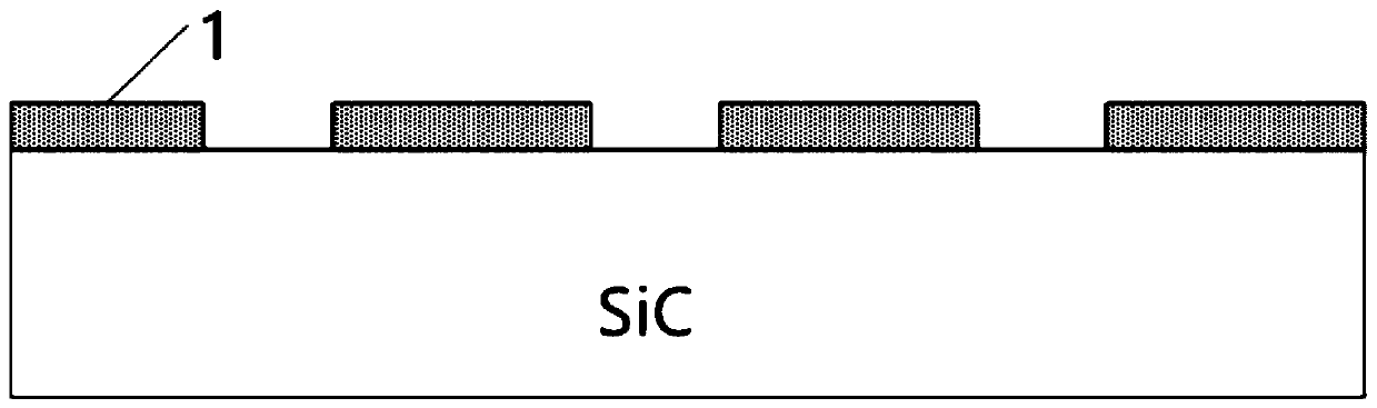
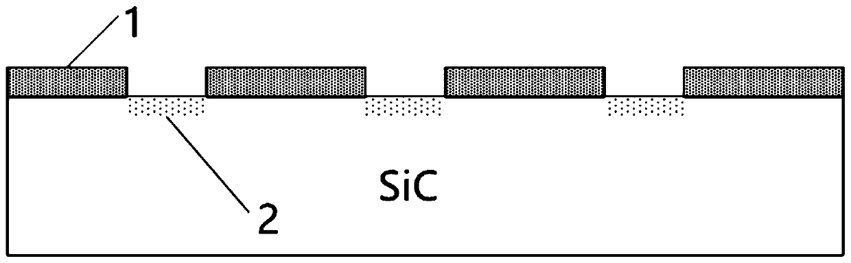
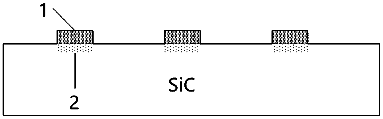
[0033] Such as Figure 1 to Figure 5 Shown is a schematic diagram of the SiC single crystal or epitaxial wafer structure shown according to the steps of preparing the gate oxide layer in the embodiment of the present invention; t...


PUM


Abstract

The invention discloses a manufacturing method of a SiC power device chip gate oxide layer and a power device. According to the manufacturing method of the gate oxide layer of the SiC power device chip, the number of introduced elements can be accurately controlled through multiple times of injection, a defect elimination effect is guaranteed, and gate reliability reduction caused by introductionof excessive P / B elements is avoided. And element distribution is optimized through multiple times of injection so that a P injection layer is completely consumed in a thermal oxidation process. An injection region is defined through photoetching before thermal oxidation, a P / B injection region is formed on a surface of an SIC, P and N elements jointly form an interface trap, an interface state isreduced, two elements are introduced without NO atmosphere annealing, the interface state is compositely reduced, the reliability of a gate is improved, and manufacturing cost of the device is reduced.

Description

technical field [0001] The invention belongs to the technical field of semiconductor chip manufacturing technology, and in particular relates to a method for manufacturing a chip gate oxide layer of a SiC power device and the power device. Background technique [0002] Silicon carbide (SiC) material is the third-generation wide-bandgap semiconductor material developed after the first-generation elemental semiconductor material (Si) and the second-generation compound semiconductor material (GaAs, GaP, InP, etc.). Due to the characteristics of wide band gap, high critical breakdown electric field, high thermal conductivity, and high electron saturation drift velocity, SiC materials are especially suitable for making microwave high-power, high-voltage, high-temperature, and radiation-resistant electronic devices, and have a wide range of applications in all aspects of the national economy. application. At present, the development of SiC devices has become a research hotspot. ...

Claims


Application Information

Patent Timeline
Patent Type & Authority Applications(China)
IPC IPC(8): H01L21/28H01L21/02H01L29/423H01L21/265
CPCH01L21/28158H01L21/02164H01L29/42364H01L21/265
Inventor 吴苏州高莹李晓云叶怀宇张国旗
Owner SOUTH UNIVERSITY OF SCIENCE AND TECHNOLOGY OF CHINA
Why Eureka
Try Eureka