TVS protection device based on P-type SOI substrate, and manufacturing method thereof

A technology for protecting devices and substrates, applied in the direction of electric solid-state devices, semiconductor devices, electrical components, etc., can solve the problem that leakage current and capacitance cannot increase significantly, circuit power consumption increases, and high-frequency signal transmission is prone to abnormalities, etc. problem, to achieve the effect of low capacitance value, lower clamping voltage, and increased contact area

Pending Publication Date: 2020-04-17
SHANGHAI CHANGYUAN WAYON MICROELECTRONICS
View PDF2 Cites 2 Cited by
  • Summary
  • Abstract
  • Description
  • Claims
  • Application Information

AI Technical Summary

Problems solved by technology

[0005] At present, with the continuous development of integrated circuits IC in the direction of miniaturization, low voltage, and low power consumption, corresponding performance requirements are also put forward for the corresponding TVS protection devices, that is, the clamping voltage of TVS is required to be as low as possible, and the leakage current And capacitance can not be significantly increased, because the increase in leakage current will lead to an increase in the power consumption of the entire circuit. When the capacitance is large, the high-frequency signal is prone to abnormalities in the transmission process.

Method used


Image

  • TVS protection device based on P-type SOI substrate, and manufacturing method thereof
  • TVS protection device based on P-type SOI substrate, and manufacturing method thereof
  • TVS protection device based on P-type SOI substrate, and manufacturing method thereof

Examples


Embodiment Construction

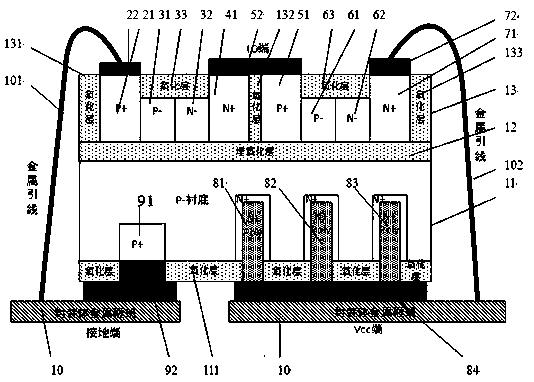
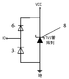
[0070] Such as figure 1 , a schematic diagram of the structure of a TVS protection device on a P-type SOI substrate and figure 2 , as shown in the equivalent circuit diagram of the TVS protection device on the P-type SOI substrate,

[0071] A TVS device, comprising a P-type SOI (Silicon-On-Insulator is on an insulating substrate) silicon wafer, a P-region, an N-region, a P+ region, an N+ region, a groove isolation oxide layer, an oxide layer, N+Poly, front metal, back metal, package metal frame, metal leads, such as figure 1 shown.

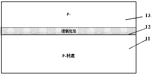
[0072] A TVS protection device based on a P-type SOI substrate, using an SOI substrate silicon wafer 1, packaged by a metal frame 10, the SOI substrate is a P-type SOI substrate 1, including from bottom to top P-substrate 11, buried oxide layer 12 and P-layer 13, wherein,

[0073] In the P-layer 13, there are first oxide layer deep groove 131, first P+ region 21, first P-region 31, first N-region 32, first N+ region 41, second oxide layer dee...


PUM

PropertyMeasurementUnit
electrical resistivityaaaaaaaaaa
thicknessaaaaaaaaaa
thicknessaaaaaaaaaa

Abstract

The invention discloses a TVS protection device based on a P-type SOI substrate. According to the device, a P-type SOI substrate silicon wafer is adopted, and is packaged by a metal frame; a P-type SOI substrate comprises a P-substrate, an oxide buried layer and a P-layer from bottom to top, has three ends of an IO end, a VCC end and a grounding end, and can protect the IO signal end and the powersupply VCC end in a circuit at the same time; a first capacitance reducing diode and a second capacitance reducing diode on the P-layer are formed by P-/N-junctions on the front surface; and a main TVS8 pipe is formed by three N+/P-substrate arrays on the back surface. According to the invention, the device is manufactured on the front side and the back side at the same time, so that the layout area of the single device is small so as to easily improve the yield and reduce the cost; the two capacitance reducing diodes have low capacitance values, and completely eliminates the substrate parasitic capacitance, so that the device is suitable for being used in high-frequency interfaces such as HDMI2.0, USB3.0 and other high-speed ports; and large surge current can pass through the TVS pipe onthe back surface.

Description

technical field [0001] The invention relates to the technical field of semiconductor protection devices, in particular to the field of design and manufacture of protection devices in SOI technology. Background technique [0002] The transient voltage suppressor (TVS device) is a clamp overvoltage protection device, which can fix the surge voltage at a relatively low voltage level in a short period of time, so that the back-end integrated circuits are protected from over-surge Voltage shocks to avoid damage. TVS devices are mainly used in various interface circuits, such as mobile phones, tablets, TV sets, and computer hosts. After the voltage enters from the IO terminal of the circuit, it will trigger the TVS device to be turned on preferentially, and the surge current will be released to the ground through the TVS device, clamping the surge voltage at a lower level, thereby protecting the back-end IC device. [0003] For example, the applicant's patent number: 20151088662...

Claims


Application Information

Patent Timeline
Patent Type & Authority Applications(China)
IPC IPC(8): H01L29/06H01L27/02
CPCH01L27/0248H01L29/0603H01L29/0684
Inventor 蒋骞苑苏海伟赵德益赵志方吕海凤张啸王允张彩霞
Owner SHANGHAI CHANGYUAN WAYON MICROELECTRONICS
Why Eureka
Try Eureka