Crystalline silicon battery assembly containing quantum cutting coating and preparation method thereof
A technology of quantum tailoring and crystalline silicon cells, applied in electrical components, circuits, photovoltaic power generation, etc., can solve the problems of silicon solar cell efficiency loss, difficulty in improving the efficiency of crystalline silicon components, and loss of crystalline silicon cell efficiency, so as to improve light energy Conversion efficiency, rich colors, effects suitable for mass production
- Summary
- Abstract
- Description
- Claims
- Application Information
AI Technical Summary
Problems solved by technology
Method used
Image
Examples
Embodiment 1
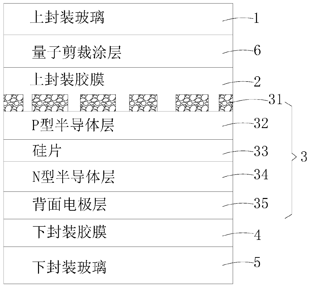
[0029] Please refer to figure 1 As shown, the first preferred embodiment of the crystalline silicon cell assembly containing the quantum tailoring coating of the present invention includes an upper encapsulating glass 1, an upper encapsulating adhesive film 2, a crystalline silicon assembly 3, and a lower encapsulating adhesive film 4 arranged up and down in sequence. and lower encapsulation glass 5 . The upper encapsulation film 2 is located on the light incident surface side of the crystal silicon component 3 . A quantum tailoring coating 6 is provided between the upper packaging glass 1 and the upper packaging adhesive film 2 . The quantum tailoring layer 6 contains perovskite quantum dot material. The perovskite quantum dot material converts visible light irradiated on the surface of the crystalline silicon component into infrared light that can be absorbed by the crystalline silicon component arranged below it.
Embodiment 2
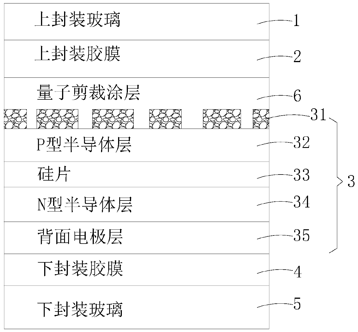
[0031] Please refer to figure 2 As shown, the second preferred embodiment of the crystalline silicon cell assembly containing the quantum tailoring coating of the present invention includes an upper encapsulating glass 1, an upper encapsulating adhesive film 2, a crystalline silicon assembly 3, and a lower encapsulating adhesive film 4 arranged up and down in sequence. and lower encapsulation glass 5 . The upper encapsulation film 2 is located on the light incident surface side of the crystal silicon component 3 . A quantum tailoring coating 6 is provided between the upper encapsulation film 2 and the crystalline silicon component 3 . The quantum tailoring layer 6 contains perovskite quantum dot material. The perovskite quantum dot material converts visible light irradiated on the surface of the crystalline silicon component into infrared light that can be absorbed by the crystalline silicon component arranged below it.
[0032] In the foregoing embodiment 1 and embodiment...
Embodiment 3
[0038] The first method for preparing a crystalline silicon cell assembly containing a quantum tailoring coating of the present invention comprises the following steps:
[0039] (11) Synthesis of cesium oleate precursor:
[0040]Mix 1g of cesium carbonate, 5mL of oleic acid and 100mL of oleylamine together, stir evenly and heat at 120°C for 30min, vacuumize the reaction system for three consecutive times, change nitrogen, and remove water vapor and Oxygen, react in an inert environment for 10 minutes, until the reaction solution becomes clear, cesium carbonate and oleic acid react completely. It is then stored in an inert environment for subsequent synthesis of quantum dots.
[0041] (12), synthetic cesium lead iodide (CsPbI 3 ) perovskite quantum dot polymer:
[0042] Another 2 g of lead iodide and 100 mL of oleylamine were thoroughly mixed, and the temperature of the reaction system was raised to 120° C. for 1 h. Then nitrogen gas was filled in the reaction system. Then...
PUM
 Abstract
Description
Claims
Application Information


