
Manufacturing method of active matrix color display device

A color display device, active matrix technology, applied in semiconductor/solid-state device manufacturing, electric solid-state devices, semiconductor devices, etc., can solve problems such as easy crosstalk, reduced utilization of LED materials, and complicated wiring.

Active Publication Date: 2020-04-21
潘小和
View PDF3 Cites 7 Cited by
  • Summary
  • Abstract
  • Description
  • Claims
  • Application Information

AI Technical Summary

Problems solved by technology

However, it is still unable to overcome the inherent defects of the passive driving method: the wiring is complex, easy to crosstalk, and the pixel strobe signal cannot be saved, etc.; in the active driving method, each LED pixel unit has its corresponding independent driving circuit, and the driving current is controlled by the driving transistor. Provide, stronger drive capability can achieve larger area drive, better brightness uniformity and contrast, can achieve low power consumption, high efficiency, high independent controllability and higher resolution, so in large area LED display Active drive is mainly used in the application
With the development of LED miniaturization and matrix technology, it is possible to integrate high-density micro-sized LED arrays on a chip, but the main problems lie in the multiple transfers, full-color, yield and luminescence of nano-scale LEDs. wavelength consistency, etc.
The biggest bottleneck is mass transfer. At present, there are many transfer solutions for mass transfer, including Pick&Place transfer, fluid assembly, laser transfer, and roller transfer. There is a big problem
Moreover, for the mass transfer of color display devices, there will be a large amount of etching technology on the LED material, thus resulting in a lot of reduction in the utilization rate of the LED material.

Method used


Image

  • Manufacturing method of active matrix color display device
  • Manufacturing method of active matrix color display device
  • Manufacturing method of active matrix color display device

Examples


Embodiment Construction

[0033]The application will be further described in detail below in conjunction with the accompanying drawings and embodiments. It should be understood that the specific embodiments described here are only used to explain related inventions, rather than to limit the invention. It should also be noted that, for the convenience of description, only the parts related to the related invention are shown in the drawings.

[0034] It should be noted that, in the case of no conflict, the embodiments in the present application and the features in the embodiments can be combined with each other. The present application will be described in detail below with reference to the accompanying drawings and embodiments.

[0035] Generally, the process of using LEDs for backlight and display includes: LED chip manufacturers arrange LED chips on blue film after production, testing and sorting, and ship them to downstream module manufacturers. Downstream module manufacturers (for example, panel ma...


PUM


Abstract

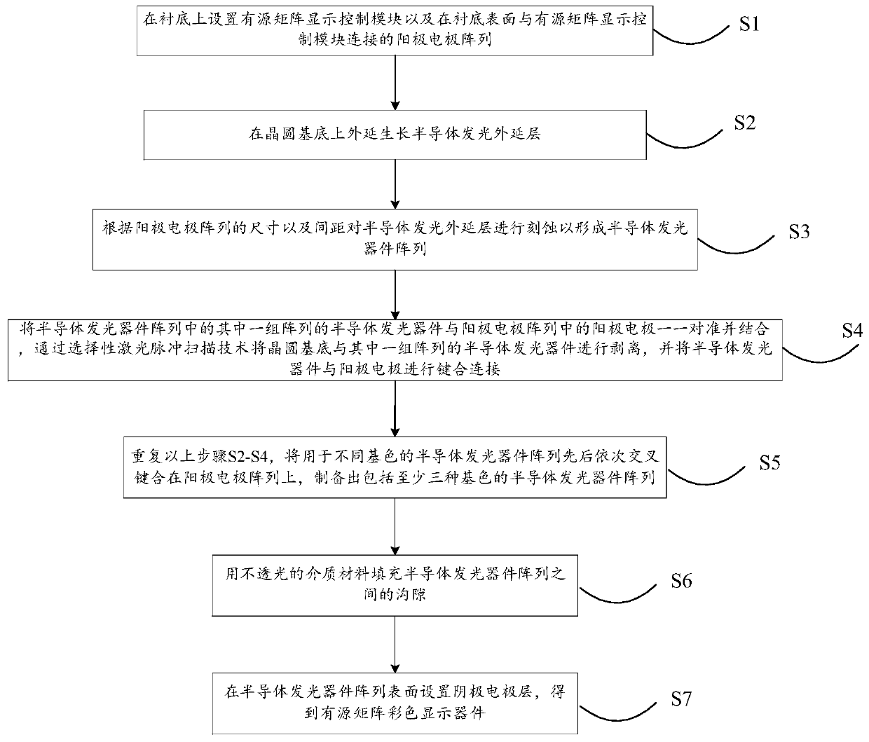
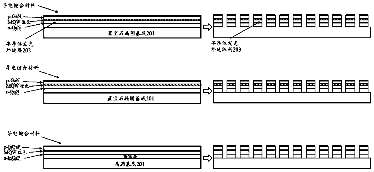
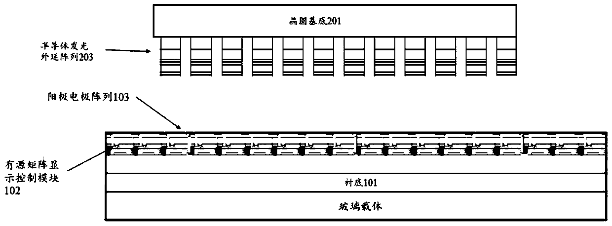
The invention discloses a manufacturing method of an active matrix color display device, which comprises the steps of arranging an active matrix display control module on a substrate and an anode electrode array connected with the active matrix display control module on surface of the substrate; epitaxially growing a semiconductor light-emitting epitaxial layer on a wafer substrate; etching to form a semiconductor light-emitting device array; aligning and combining the semiconductor light-emitting devices of one group of arrays in the semiconductor light-emitting device array with the anode electrodes in the anode electrode array in a one to one manner, and stripping and bonding the wafer substrate and the semiconductor light-emitting devices of one group of arrays through a selective laser pulse scanning technology; repeating the above steps, and sequentially bonding the semiconductor light-emitting device arrays for different primary colors on the anode electrode array in a crossed manner; filling a trench gap between the semiconductor light-emitting devices; and arranging a cathode electrode layer on the surface of the semiconductor light-emitting device array. The utilization rate of the semiconductor light-emitting epitaxial layer is improved by three times through the selective laser scanning technology.

Description

technical field [0001] The embodiments of the present application relate to the display field, and in particular to a method for manufacturing an active matrix color display device. Background technique [0002] At present, more and more attention has been paid to display devices based on the principle that light emitting diodes (Light Emitting Diodes) form pixel units for display, which mainly include organic light emitting diodes (OLEDs), small-pitch LEDs, mini light emitting diodes (Mini LED), micro light emitting diode (Micro LED) and quantum dot light emitting diode (QLED), etc. This type of LED-based display technology has the advantages of self-illumination without backlight, low power consumption, high brightness, long life, and fast response. It can be applied to small and medium-sized display screens such as mobile phones, tablet computers, and wearable devices. Therefore, received widespread attention. [0003] Existing LED display devices are current-driven lig...

Claims


Application Information

Patent Timeline
IPC IPC(8): H01L25/16H01L25/00H01L21/18
CPCH01L25/167H01L25/50H01L21/187
Inventor 潘小和
Owner 潘小和
Learn More