Quantum dot material, preparation method and application thereof, and light-emitting device
A technology for quantum dot materials and light-emitting devices, applied in the field of quantum dots, can solve the problems of many surface defects, uneven size, insufficient luminous efficiency, etc., and achieve the effects of uniform square resistance, low square resistance, and improved luminous efficiency.
- Summary
- Abstract
- Description
- Claims
- Application Information
AI Technical Summary
Problems solved by technology
Method used
Image
Examples
Embodiment 1
[0039] A preparation method of sodium-doped indium phosphide quantum dots, specifically comprising the following steps:
[0040] (1) Take 0.1 mmol of anhydrous indium acetate and 0.15 mmol of anhydrous sodium acetate and dissolve them in acetic acid / n-butanol solution (the mass fraction of glacial acetic acid is 50%) to obtain solution 1;
[0041] (2) Disperse tris(trimethylsilyl)-phosphine at a concentration of 10 mmol / L in acetic acid / n-butanol solution (the mass fraction of glacial acetic acid is 50%) to obtain solution 2;
[0042] (3) Drop solution one into solution two under high-speed stirring (400-1000rpm), and then stir at high speed for 2 hours;
[0043] (4) Pour the mixed solution into a microwave reactor, put it into a microwave reactor, and react with microwave at 120° C. for 5 hours;
[0044](5) After cooling, take out the reaction kettle, put it in the vacuum oven, heat it up to 120°C after vacuuming, and after evaporating 3 / 4 of the volume of liquid, pour it ba...
Embodiment 2
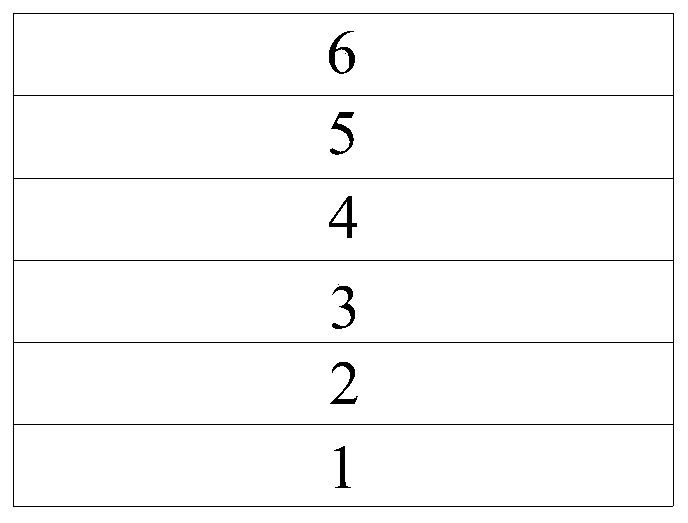
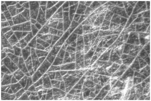
[0068] A light-emitting device, the difference from Example 1 is that the obtained nano-silver wire-graphene composite conductive film is cut, the circuit is etched, a solder resist is pasted, and the IC chip and the resistance element are packaged with epoxy resin. Finally, it is laminated with the above-mentioned light-emitting combination layer (hole injection layer, hole transport layer, quantum dot layer, electron injection layer, electron transport layer) and sealed with epoxy resin.
Embodiment 3
[0070] A kind of cesium doped indium phosphide quantum dot, its structural formula is Cs 3 In 2 P 3 .
[0071] The preparation method of the quantum dot material comprises the following steps:
[0072] (1) Take 0.1 mmol of anhydrous indium acetate and 0.15 mmol of anhydrous cesium acetate and dissolve them in 50% acetic acid / n-butanol solution to obtain solution 1;
[0073] (2) Disperse tris(trimethylsilyl)-phosphine in 50% acetic acid / n-butanol solution at a concentration of 10 mmol to obtain solution 2;
[0074] (3) Drop solution one into solution two under high-speed stirring state, and then stir at high speed for 2 hours;
[0075] (4) Pour the mixed solution into a microwave reactor, put it into a microwave reactor, and react with microwave at 120° C. for 5 hours;
[0076] (5) Take out the reaction kettle after cooling, and put it in a vacuum oven, heat it up to 120°C after vacuuming, and after evaporating 3 / 4 of the liquid, pour it back into the ethylene glycol / n-but...
PUM
| Property | Measurement | Unit |
|---|---|---|
| diameter | aaaaa | aaaaa |
| length | aaaaa | aaaaa |
| radius | aaaaa | aaaaa |
Abstract
Description
Claims
Application Information
 - R&D
- Intellectual Property
- Life Sciences
- Materials
- Tech Scout
- Unparalleled Data Quality
- Higher Quality Content
- 60% Fewer Hallucinations
Browse by: Latest US Patents, China's latest patents, Technical Efficacy Thesaurus, Application Domain, Technology Topic, Popular Technical Reports.
© 2025 PatSnap. All rights reserved.Legal|Privacy policy|Modern Slavery Act Transparency Statement|Sitemap|About US| Contact US: help@patsnap.com


