DJ type two-dimensional double-layer hybrid perovskite material, preparation method thereof and application of perovskite material
A perovskite material and double-layer technology, applied in the field of photoelectric detection, can solve problems such as poor performance and slow response speed, and achieve the effects of high thermodynamic stability, low dark current, and high stability
- Summary
- Abstract
- Description
- Claims
- Application Information
AI Technical Summary
Problems solved by technology
Method used
Image
Examples
Embodiment 1
[0029] Step 1, 20mL HI (47%) solution containing lead acetate (0.758g, 2mmol) and methylamine (0.031g, 1mmol) was heated and stirred for 15min, then naturally cooled to room temperature, and evaporated slowly. After 4 days, red flaky crystals were obtained .
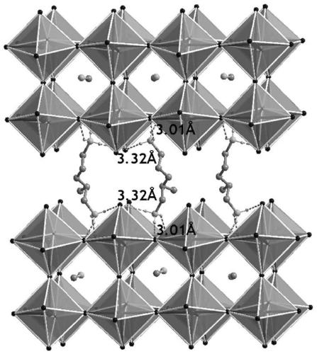
[0030] Step 2, under the condition of heating and stirring, dissolve the red flaky crystal obtained in step (1) in HI solution, then add 2-methyl-1,5-pentanediamine (0.116g, 1mmol), heat and stir After the solution became clear, it was naturally cooled to room temperature and evaporated slowly. After 7 days, dark red blocky crystals were obtained. This crystal is the described (2-methyl-1,5-pentanediamine) (methylamine) Pb 2 I 7 Material. The crystal structure was obtained by X-ray single crystal diffractometer analysis, such as figure 1 shown.
Embodiment 2
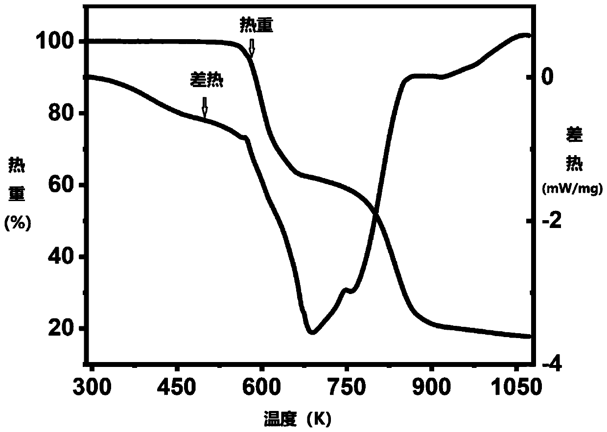
[0032] (2-Methyl-1,5-pentanediamine)(methylamine)Pb 2 I 7 Thermogravimetric analysis of crystalline materials.
[0033] The thermogravimetric analysis of the crystal material obtained in Example 1 shows that the material has high thermal stability and can be stably used below 272°C.
Embodiment 3
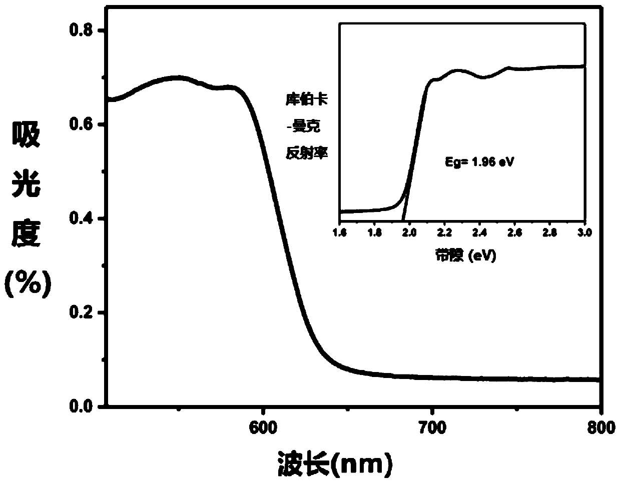
[0035] (2-Methyl-1,5-pentanediamine)(methylamine)Pb 2 I 7 The light-absorbing ability of the crystal material was analyzed, and the ultraviolet-visible absorption spectrum test was carried out on the synthesized organic-inorganic hybrid material. from image 3 We can obtain that the light absorption range of the material reaches 630nm, while the ultraviolet-visible light absorption range is 200-780nm, so the crystal material meets the requirement of being a high absorption semiconductor material.
PUM
 Abstract
Description
Claims
Application Information
 - R&D Engineer
- R&D Manager
- IP Professional
- Industry Leading Data Capabilities
- Powerful AI technology
- Patent DNA Extraction
Browse by: Latest US Patents, China's latest patents, Technical Efficacy Thesaurus, Application Domain, Technology Topic, Popular Technical Reports.
© 2024 PatSnap. All rights reserved.Legal|Privacy policy|Modern Slavery Act Transparency Statement|Sitemap|About US| Contact US: help@patsnap.com


