
Local plating resistance protective method of SOP packaged to-be-plated circuit module

A circuit module and plating resist technology, applied in the field of local resist plating protection of the circuit module to be plated, can solve the problems of increased adhesion, corrosion of outer leads, influence of solderability, etc., to prevent insufficient strength, short curing time, Combine good results

Inactive Publication Date: 2020-06-02
XIAN MICROELECTRONICS TECH INST
View PDF3 Cites 0 Cited by
  • Summary
  • Abstract
  • Description
  • Claims
  • Application Information

AI Technical Summary

Problems solved by technology

[0004] Before the metallization of the surface of the SOP package circuit module, the non-plating area needs to be protected to achieve the purpose of partial surface metallization. However, due to the complex structure of the non-plating area of ​​the circuit module, it is necessary to protect the two rows of outer leads vertically drawn from the bottom of the module and the surface of the bottom plate. , the use of ordinary protection methods, such as making special resist plating jigs, coating resist glue, wrapping resist tape and other processes cannot achieve the resist plating effect, which is likely to cause plating solution leakage; and use resist plating paint with strong adhesion Protection will cause the lead area to be uncleanly removed and chemical reagents will damage the solder resist on the bottom plate, etc., which will affect the solderability and appearance of the final product
The traditional method of resisting plating cannot be applied to the resisting protection of this circuit, and there are mainly the following problems:
[0005] 1. Plating-resisting peelable adhesive coating: The resisting-plating peelable adhesive has a high viscosity, and there will be individual bubbles and pores in the direct application process, and the plating solution will still leak and cause corrosion to the non-plating area; and increasing the number of coatings will inevitably make The adhesive layer becomes thicker, and the adhesive force is significantly increased, which will cause damage such as distortion and deformation of the outer lead during the subsequent removal process
[0006] 2. Covering and protection of plating-resisting fixtures and fixtures: Due to the small size of the circuit module and the high height of the stand, it is necessary to use external leads to achieve cathode electrical conduction during the surface metallization process (such as figure 2 ), the tooling needs to be slotted with a depth-to-width ratio greater than 40:1, and it is necessary to add electrical connection points in the groove with a width of about 0.4-0.5 mm, and it is necessary to make clamping points during the surface metallization process. The tooling is more difficult to realize Big
Moreover, there are many types of products and different packaging sizes. A large number of tooling needs to be produced for each product, which is not conducive to cost control.
[0007] 3. Coating of resisting paint: The surface metallization of SOP packaged circuit modules needs to electrolessly plate a layer of nickel on the surface of the epoxy potting compound, and in the process of electroless nickel plating, the surface of the resisting paint will be plated with a nickel layer. When the organic solvent removes the resist plating paint, due to the barrier of the nickel layer on the surface, the resist plating paint and the organic solvent cannot chemically react, and the resist plating paint cannot be removed
On the other hand, because the surface metallization process is long and the composition of the plating solution is complex, the pH range of the plating solution in the whole process is: 0.2 to 11, and it is necessary to use a resisting paint that is resistant to acid and alkali corrosion, and this kind of resisting paint must be used. Strong organic solvents are used to remove them. Long-term immersion in organic solvents will cause damage to the epoxy glue of the potting body and the solder resist paint on the bottom plate. Therefore, the plating resist protection of the circuit cannot be achieved by only using the resist plating paint.
[0008] Based on this, our research group has previously improved the plating resist protection method. Specifically, first wrap the plating resist tape on the side of the outer lead, then place a clamp between the two outer leads, and finally apply the resist plating on the non-metallized area to protect it. However, when this method is used to wrap the plating resist tape on the side of the outer lead, if the protective area of ​​the plating resist tape is too large, the distance between the upper edge of the plating resist tape and the conductive clamping hole is too small, and the plating resist can be applied. When peeling the glue, in order to ensure the permeability of the conductive clamping hole, the protection of the plating resist tape on the surface of the outer lead is not complete. During the surface metallization process, the plating solution penetrates from the gap of the plating resist tape; and Since the distance between the outside of the outer lead and the edge of the circuit module is generally about 1 mm, there will be glue adhered to the surface to be plated during the process of applying the resist-plating peelable adhesive. The excess adhesive layer on the surface, because the resist-plating peelable adhesive liquid adheres to the surface as a whole after curing, in the process of eradicating, it will generate tension on the adhesive layer adhered to the surface of the bottom plate, and the contact area is small (the resist-plating tape will be wound after winding. The area where the resist plating can be stripped and the thickness of the base plate is only about 0.5mm) is separated from the base plate, resulting in the lack of tight plating protection and the penetration of the plating solution, while the plating resist tape wrapped around the outer lead is only for a single outer lead. The two outer surfaces of the lead are protected, and there is no protection for the two surfaces of a single lead. Once the plating solution leaks, the surface of the lead will be electroplated with excess plating, resulting in poor appearance or even affected solderability; or acid plating liquid infiltration, corrosion of the external leads, and cracking of the lead base material when the lead is bent and formed in later products

Method used


Image

  • Local plating resistance protective method of SOP packaged to-be-plated circuit module
  • Local plating resistance protective method of SOP packaged to-be-plated circuit module
  • Local plating resistance protective method of SOP packaged to-be-plated circuit module

Examples


Embodiment 1

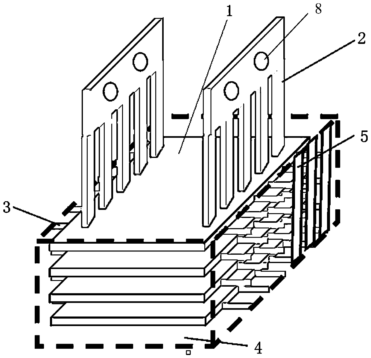
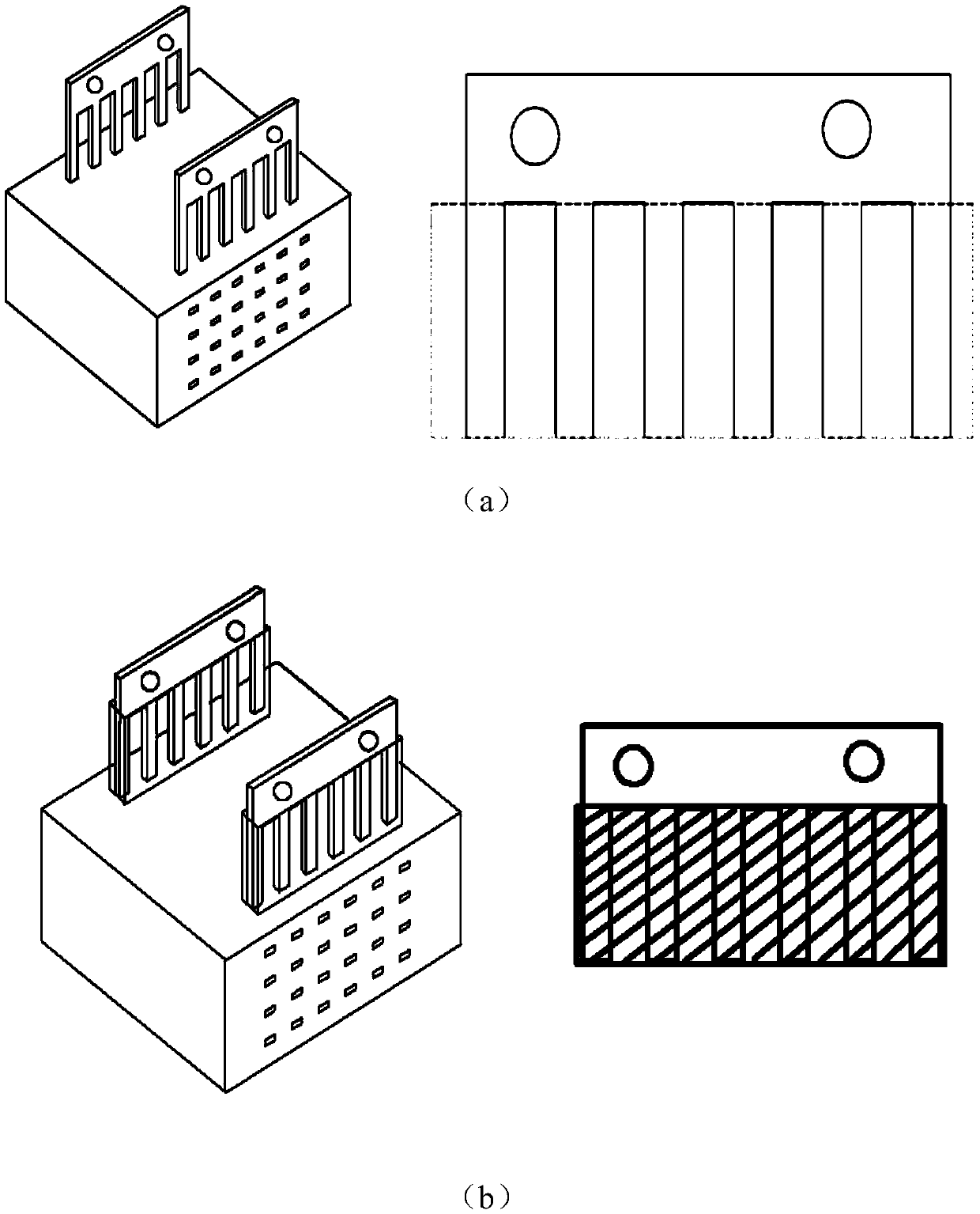
[0047] Step 1. Apply anti-corrosion glue on the outer lead: dip a small amount of anti-corrosion glue with a fine hook line pen and apply it along the direction of the outer lead 2 from bottom to top to ensure that the leakage part of the outer lead 2 is protected.

[0048] Step 2. Baking and curing in oven: temperature is 80℃, time is 60min.

[0049] Step 3. Protect the outer lead with plating resist tape: Wrap a layer of plating resist tape with the same width as the height of the comb-shaped area of ​​outer lead 2 along the side of outer lead 2. Put it in an oven to heat: temperature 80℃, time 10min, flattened with bamboo Use tweezers to compact and adhere the plating resist tape along the outer lead 2 direction.

[0050] Step 4, bonding and fixing the clamp block: fix the clamp block 6 on the bottom plate 1 between the two outer leads 2 with non-transferring tape, ensure that the width of the clamp block 6 matches the span of the outer lead 2, and the length of the clamp block 6 ...

Embodiment 2

[0058] The difference from Example 1 is: the baking temperature of step 2 is 75° C. and the time is 55 min; the oven heating temperature of step 3 is 75° C. and the time is 55 min; step 6 is naturally dried for 13 h; and step 9 is soaked in solvent for 2 min.

Embodiment 3

[0060] The difference from Example 1 is that the baking temperature in step 2 is 85° C. and the time is 65 min; the oven heating temperature in step 3 is 85° C. and the time is 65 min; step 6 is naturally dried for 14 hours; and step 9 is soaked in solvent for 3 min.


PUM


Abstract

The invention provides a local plating resistance protective method of an SOP packaged to-be-plated circuit module. The local plating resistance protective method comprises the following steps: 1, painting corrosion resistant adhesive on the surface of an outer lead, and baking for curing; 2, wrapping a layer of plating resistance adhesive tape along the side face of the outer lead, wherein the width of the plating resistance adhesive tape is the same as the height of a comb shaped area of the outer lead; 3, bonding and fixing a fixture block on the upper surface of a bottom plate between twoouter leads to enable the fixture block to cover the surface of the bottom plate between two outer leads; 4, painting plating resistance peelable glue on the exposed side face of the outer lead, the exposed side face and top surface of the fixture block and the exposed upper surface of the bottom plate, and airing; 5, adopting chemical nickle plating and electroplating nickel-gold for surface metallization; 6, peeling off the plating resistance peelable glue and removing the fixture block and the plating resistance adhesive tape; and 7, adopting organic solvent capable of dissolving corrosionresistant adhesive to remove the corrosion resistant adhesive. Through combination of multiple materials and technologies, the bottom plate of the circuit module and the two rows of outer leads are not corroded during the surface metallization process.

Description

Technical field [0001] The invention relates to electronic electroplating, in particular to a method for partial resistance plating protection of a SOP packaged circuit module to be plated. Background technique [0002] The SOP package circuit module is to vertically stack the packaged device, two-dimensional interconnection layer and outer leads, and then use epoxy resin potting compound for overall potting. After curing, the side of the potting body is accurately cut to form an interconnection point matrix , And then form side interconnection lines through surface metallization and laser scribing to complete the three-dimensional assembly and interconnection of the packaged devices. The surface metallization is the key condition to realize the interconnection point connection. [0003] The schematic diagram of the SOP package circuit module structure is as figure 1 As shown, the bottom plate 1 is a screen-printed solder resist on the surface of the FR-4 printed board, and the ou...

Claims


Application Information

Patent Timeline
IPC IPC(8): C25D5/02C23C18/32C25D3/12C25D3/48C23C28/02H01L21/48
CPCC23C18/1605C23C18/32C23C28/023C25D3/12C25D3/48C25D5/02H01L21/4885H01L21/4889
Inventor 陈慧贤顾毅欣张丁
Owner XIAN MICROELECTRONICS TECH INST
Learn More