Inversion perovskite solar cell containing alkali metal halide hole modification layer and preparation method thereof
A technology of alkali metal halides and solar cells, applied in the field of solar cells, can solve the problems of difficult large-scale preparation and commercialization, incomplete coverage of perovskites, and limited battery performance, achieving low cost, improved performance, The effect of improving overall performance
- Summary
- Abstract
- Description
- Claims
- Application Information
AI Technical Summary
Problems solved by technology
Method used
Image
Examples
Embodiment 1
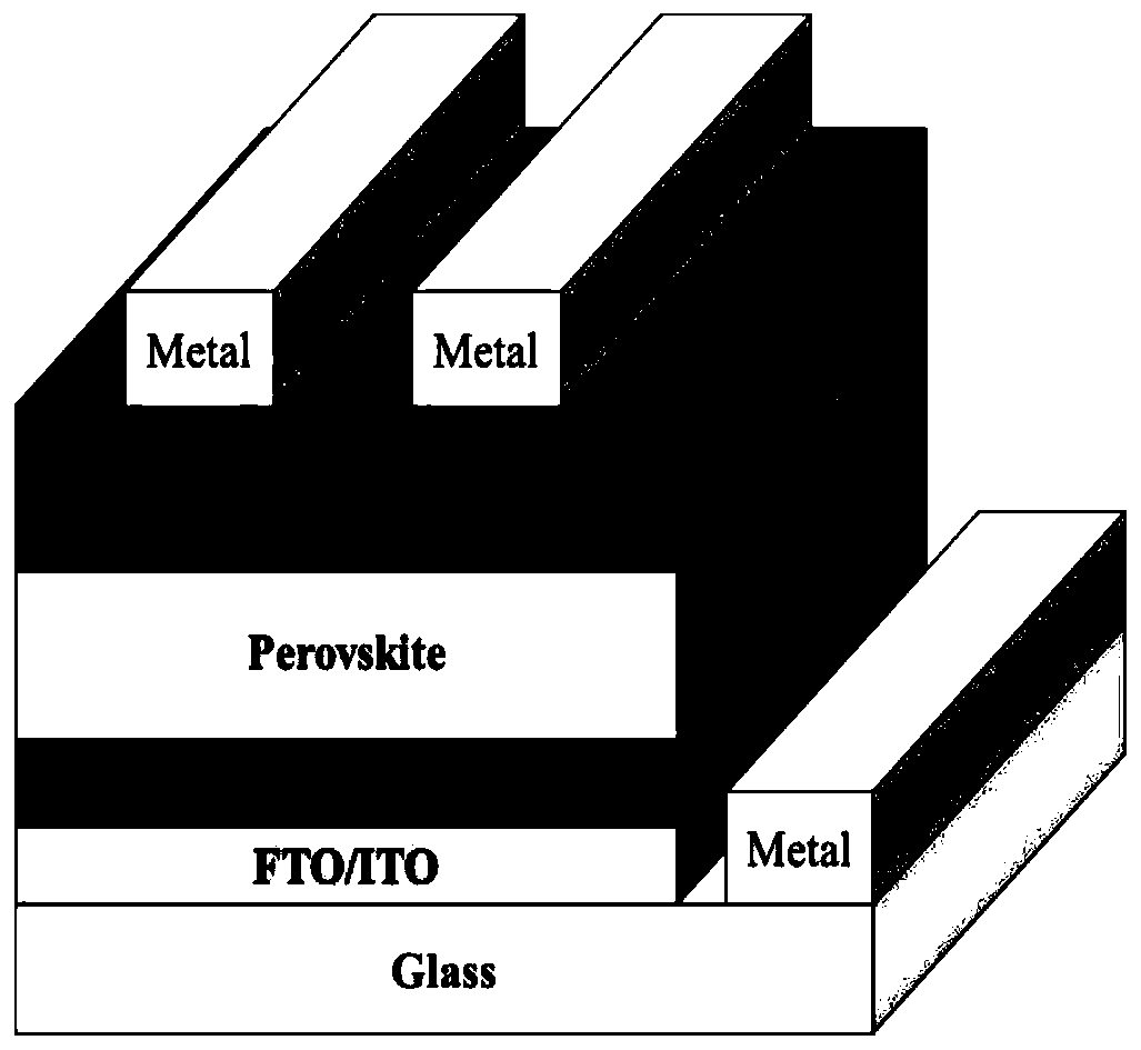
[0038] An inverse perovskite solar cell, comprising a conductive substrate, and a stacked structure arranged on part of the conductive substrate, the stacked structure includes a hole transport layer, a hole layer, and a hole transport layer stacked sequentially from bottom to top The transport layer modification layer, the perovskite light absorbing layer, the electron transport layer and the metal electrode, and a part of the metal electrode is also provided on the conductive substrate, and this part of the metal electrode is not in contact with the stacked structure.
[0039] The above conductive substrate is FTO conductive glass, the material used for the hole transport layer is nickel oxide, and the thickness of the nickel oxide is 20nm; the material used for the hole transport layer modification layer is alkali metal halide CsI, and the thickness is 25nm; the perovskite light absorbing layer The material used is CH 3 NH 3 PB 3 The perovskite light-absorbing layer has a...
Embodiment 2
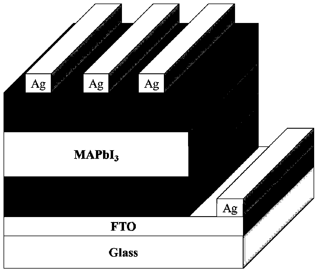
[0052] An inverse perovskite solar cell with a device structure such as figure 2 As shown, it includes a conductive substrate, and a laminated structure provided on part of the conductive substrate, the laminated structure includes a hole transport layer, a hole transport layer modification layer, a perovskite stacked sequentially from bottom to top ore light-absorbing layer, electron transport layer, electron transport layer modification layer and metal electrode, and a part of metal electrode is also provided on the conductive substrate, and this part of metal electrode is not in contact with the laminated structure.
[0053] The above conductive substrate is FTO conductive glass, the material used for the hole transport layer is nickel oxide, and the thickness of the nickel oxide is 20nm; the material used for the hole transport layer modification layer is alkali metal halide CsI, and the thickness is 25nm; the perovskite light absorbing layer The material used is CH 3 NH...
Embodiment 3
[0056] An inverse perovskite solar cell with a device structure such as figure 2 As shown, it includes a conductive substrate, a hole transport layer, a hole transport layer modification layer, a perovskite light-absorbing layer, an electron transport layer and a metal electrode that are stacked sequentially from bottom to top.
[0057] The above-mentioned conductive substrate is FTO conductive glass, the material used for the hole transport layer is nickel oxide, and the thickness of the nickel oxide is 20nm; the material used for the modification layer of the hole transport layer is alkali metal halide CsCl, and the thickness is 25nm; The material used is CH 3 NH 3 PB 3 The perovskite light-absorbing layer has a thickness of 300nm; the material used for the electron transport layer is PCBM, and the thickness is 20nm; the metal electrode is a silver electrode, and the thickness is 100nm.
[0058] The preparation process of the above-mentioned device is the same as in Exam...
PUM
| Property | Measurement | Unit |
|---|---|---|
| thickness | aaaaa | aaaaa |
| thickness | aaaaa | aaaaa |
| thickness | aaaaa | aaaaa |
Abstract
Description
Claims
Application Information


