Dislocation identification method of silicon carbide crystal

An identification method and technology of silicon carbide, which is applied in the preparation of test samples, optical test flaws/defects, etc., can solve the problems of inability to realize identification at the same time, long corrosion time, etc., to achieve accurate identification, short corrosion time, easy characterization and The effect of statistics

Pending Publication Date: 2020-06-05
SICC CO LTD
View PDF10 Cites 10 Cited by
  • Summary
  • Abstract
  • Description
  • Claims
  • Application Information

AI Technical Summary

Problems solved by technology

In this method, KOH, NaOH or a mixture of the two is used as the etchant, and the etching time is 10 to 35 minutes. This method can accurately determine the types of mixed dislocations, screw dislocations and edge dislocations in silicon carbide crystals. The identification of edge dislocation, screw dislocation and basal plane dislocation cannot be realized at the same time, and the corrosion time is long

Method used


Image

  • Dislocation identification method of silicon carbide crystal
  • Dislocation identification method of silicon carbide crystal
  • Dislocation identification method of silicon carbide crystal

Examples


Embodiment 1

[0051] Example 1: Dislocation identification method for high-purity silicon carbide

[0052] This embodiment describes a dislocation identification method for high-purity silicon carbide, the method comprising the following steps:

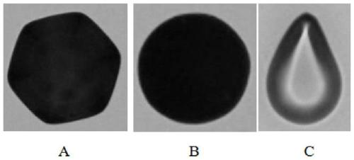
[0053] (1) Pretreatment: The high-purity silicon carbide is firstly ground and polished according to the normal process to make it have a flat and smooth surface. Then use ultrapure water to clean the crystal surface particles, dilute sulfuric acid to clean the crystal surface grease, and use hydrofluoric acid (mass concentration is 8%) to pre-corrode the crystal surface. The temperature of the pre-corrosion is 20 ° C. It is also possible to eliminate scratches on the crystal surface; finally use hydrogen peroxide and sodium bicarbonate to neutralize and clean the pretreatment solution. Then use ultra-pure water to wash and dry the wafer several times to complete the pretreatment process. The purpose of pretreatment: one is to clean the surface o...

Embodiment 2

[0057] Example 2: Dislocation identification method for high-purity silicon carbide

[0058] This embodiment describes a dislocation identification method for high-purity silicon carbide, the method comprising the following steps:

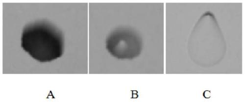
[0059] (1) Pretreatment: The high-purity silicon carbide is firstly ground and polished according to the normal process to make it have a flat and smooth surface. Then use ultra-pure water to clean the crystal surface particles, dilute hydrochloric acid to clean the crystal surface grease, and use nitric acid (mass concentration is 5%) to carry out pre-corrosion on the crystal surface. Surface scratches are eliminated and removed; finally, hydrogen peroxide and sodium bicarbonate are used to neutralize and clean the pretreatment solution. Then use ultra-pure water to wash and dry the wafer several times to complete the pretreatment process.

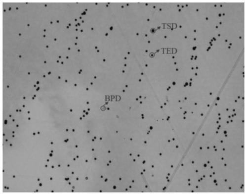
[0060] (2) Dislocation corrosion process: KOH solid particles are placed in a nickel crucible and melted ...

Embodiment 3

[0062] Example 3: Dislocation identification method for high-purity silicon carbide

[0063] This embodiment describes a dislocation identification method for high-purity silicon carbide, the method comprising the following steps:

[0064] (1) Pretreatment: The high-purity silicon carbide is firstly ground and polished according to the normal process to make it have a flat and smooth surface. Then use ultrapure water to clean the crystal surface particles, dilute sulfuric acid to clean the crystal surface grease, and use a mixture of hydrofluoric acid and nitric acid with a molar ratio of 6:1 to pre-corrode the crystal surface. The pre-corrosion temperature is 15 ℃, the mass concentration of the mixed solution of hydrofluoric acid and nitric acid is 10%, the mixed solution of hydrofluoric acid and nitric acid can also eliminate the scratches on the crystal surface; Neutralize and clean. Then use ultra-pure water to wash and dry the wafer several times to complete the pretrea...


PUM


Abstract

The invention provides a dislocation identification method of a silicon carbide crystal. The method comprises the following steps: (1) corroding the silicon carbide crystal in an alkaline corrosive agent; and (2) after the corrosion is completed, observing the morphology of a dislocation corrosion pit so as to identify blade dislocation, screw dislocation and base plane dislocation in the siliconcarbide crystal, wherein the silicon carbide crystal comprises high-purity silicon carbide and nitrogen-doped silicon carbide, the corrosion time of the high-purity silicon carbide is 5-7 minutes, andthe corrosion time of the nitrogen-doped silicon carbide is 7-9 minutes. According to the method, the corrosion time of alkaline corrosion is optimized, and the corrosion time of high-purity siliconcarbide and nitrogen-doped silicon carbide is controlled to be less than 10 minutes so that three dislocations including edge dislocations, screw dislocations and base plane dislocations in the high-purity silicon carbide or the nitrogen-doped silicon carbide can be accurately distinguished; the corrosion time is short; and three dislocations in the crystal can be accurately identified.

Description

technical field [0001] The invention relates to a method for dislocation identification of silicon carbide crystals, belonging to the technical field of test and characterization of crystal materials. Background technique [0002] As a new type of power component material, silicon carbide has attracted widespread attention because of its high resistivity, high strength and good thermal conductivity. However, due to the high requirements for its growth conditions, the defects introduced during the growth process limit the improvement of its performance and its further application and development. Therefore, the characterization and statistics of defects become the first prerequisite for improving the defects. Dislocation, as a kind of line defect, can be divided into edge dislocation (TED), screw dislocation (TSD) and basal plane dislocation (BPD) according to the difference of its formation mechanism and the difference of semi-atom plane. Different dislocations and their d...

Claims


Application Information

Patent Timeline
Patent Type & Authority Applications(China)
IPC IPC(8): G01N1/32G01N21/88
CPCG01N1/32G01N21/88
Inventor 张九阳李霞高宇晗高超
Owner SICC CO LTD
Why Eureka
Try Eureka