Circuit board, preparation method and electronic device
A circuit board and capacitor technology, applied in circuit devices, printed circuit manufacturing, multi-layer circuit manufacturing, etc., can solve problems such as poor high-frequency filtering effect of capacitors
- Summary
- Abstract
- Description
- Claims
- Application Information
AI Technical Summary
Problems solved by technology
Method used
Image

Examples
Embodiment 1
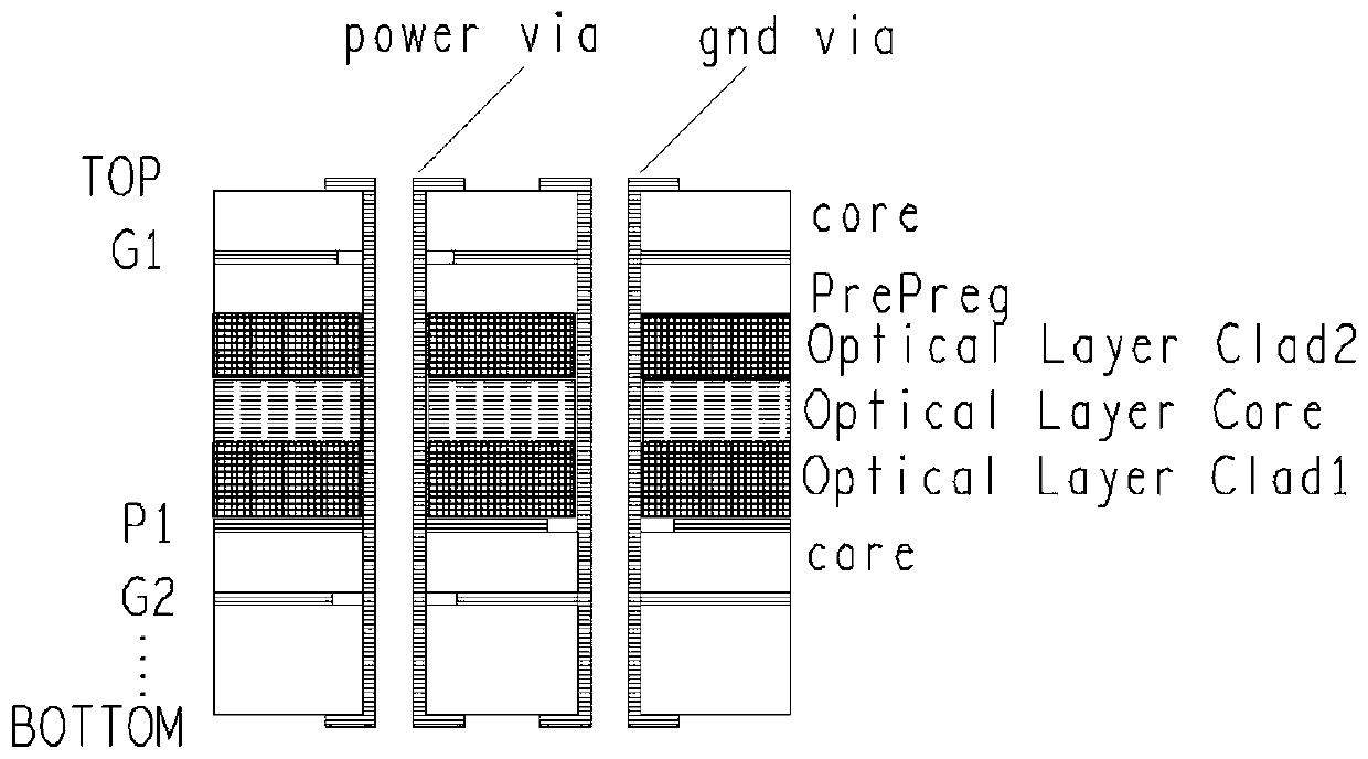
[0043] Embodiment 1 provides a circuit board, Figure 4 is a schematic structural diagram of a circuit board according to an embodiment of the present invention, such as Figure 4 As shown, the circuit board at least includes a first base layer 1, wherein, in the area of the first side of the first base layer 1, there are: a first planar capacitor group 2 and an optical waveguide 3, wherein the first planar capacitor group includes At least one pair of planar capacitors, the first planar capacitor group 2 and the optical waveguide 3 are arranged side by side along a direction parallel to the plane where the first base layer 1 is located.
[0044] Through the embodiment of the present invention, the power supply via hole on the circuit board does not need to pass through the optical waveguide layer, which greatly shortens the effective length of the power supply via hole, thereby reducing the parasitic inductance of the power supply via hole and avoiding the parasitic inducta...
specific Embodiment approach 1
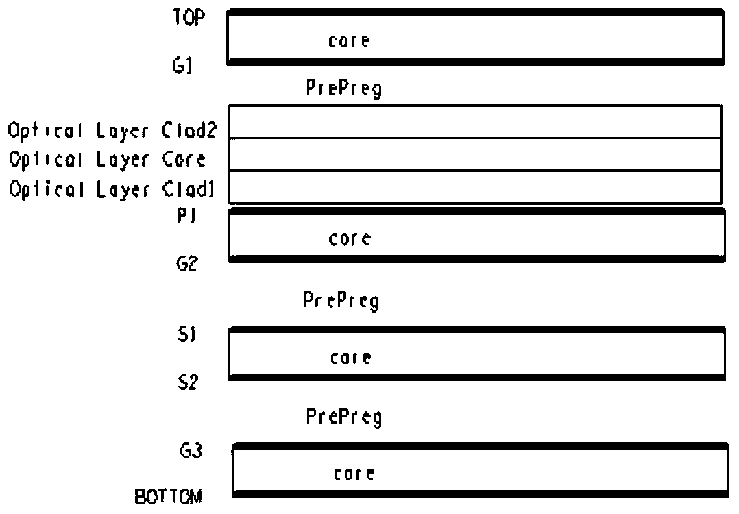
[0086] In this specific embodiment, the optical waveguide layer and the planar capacitor are structured in parallel, and the optical waveguide layer and the planar capacitor are constructed on the same substrate. The planar capacitance formed by the power plane P1 and the ground plane G1 (equivalent to the first ground plane in the above embodiment) is adjacent to the component mounting surface S, and the chip power pins only need to pass through the core board 500 and the prepreg 201 to connect to the power plane , Shorten the effective length of the power via by more than 50%. At the same time, the part of the power plane P1 corresponding to the optical waveguide is hollowed out to expose the ground plane G1, and the optical waveguide layer is constructed on the exposed ground copper (the exposed ground copper is equivalent to the first metal layer in the above embodiment). In this way, the optical waveguide layer and the mounting surface are only separated by the thickness ...
specific Embodiment approach 2
[0103] In Embodiment 2 of Embodiment 1, on the basis of the plane capacitance in Embodiment 1, a core board with one side being the power plane P2 and the other side being the ground plane G3 is added. The traffic is large, and it can also be shared by two power planes. The added core board and the optical waveguide layer are also in a parallel relationship.
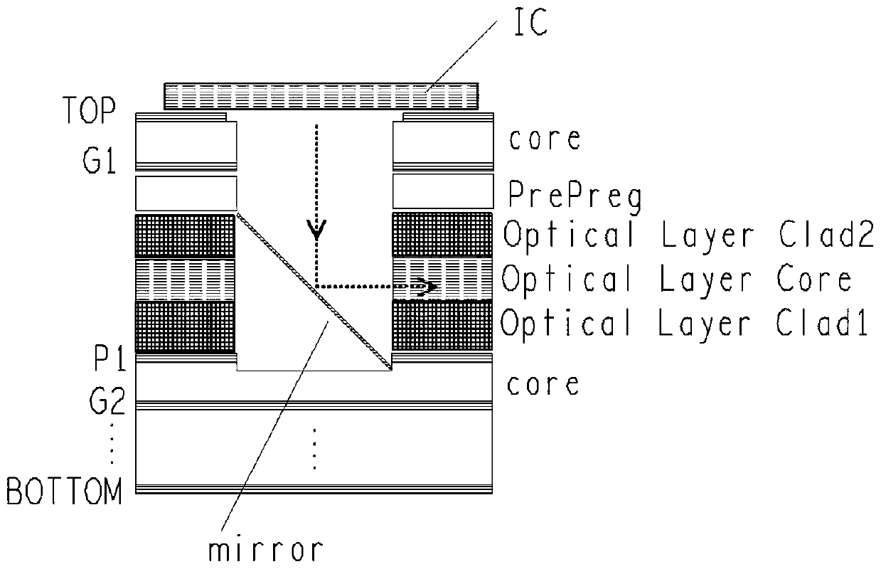
[0104] Figure 8 It is a schematic diagram of a partial structure of a circuit board according to Embodiment 2 of the embodiment of the present invention, showing the connection relationship between the electrical signal interconnection part and the optical waveguide part; Figure 9 It is a schematic diagram of the stacked structure of the electrical signal interconnection part of the circuit board according to the second embodiment of the present invention, showing the stacked structure of the electrical signal interconnection part, and the connection relationship between the ground hole and the power hole. like Fig...
PUM
 Abstract
Description
Claims
Application Information
 - R&D
- Intellectual Property
- Life Sciences
- Materials
- Tech Scout
- Unparalleled Data Quality
- Higher Quality Content
- 60% Fewer Hallucinations
Browse by: Latest US Patents, China's latest patents, Technical Efficacy Thesaurus, Application Domain, Technology Topic, Popular Technical Reports.
© 2025 PatSnap. All rights reserved.Legal|Privacy policy|Modern Slavery Act Transparency Statement|Sitemap|About US| Contact US: help@patsnap.com