

GeSbTe phase change material thin film device with high bonding capacity and low resistance
A combination ability and material thin film technology, applied in the field of phase change storage, can solve the problems affecting the conduction effect between the lower electrode layer and the first GeSbTe material layer, affecting the resistance reduction of storage devices, and affecting product consistency, so as to facilitate scale Good production and interface binding ability and good consistency
- Summary
- Abstract
- Description
- Claims
- Application Information
AI Technical Summary
Problems solved by technology
Method used
Image

Examples
Embodiment 1
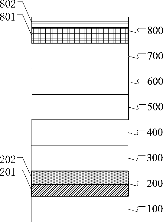
[0036] The invention discloses a GeSbTe phase-change material film device with strong binding ability and low resistance value, comprising a lower electrode layer, a first GeSbTe material layer, a molybdenum disulfide layer, a second GeSbTe material layer, a graphene layer, and an upper electrode layer And the protective layer, the lower electrode layer, the first GeSbTe material layer, the molybdenum disulfide layer, the second GeSbTe material layer, the graphene layer, the upper electrode layer, and the protective layer are sequentially arranged and superimposed on the substrate layer, and the lower electrode layer is a double layer Composite structure, the lower electrode layer includes a Cr-Ag alloy coating coated on the substrate layer and a Cr-M alloy material layer arranged on the surface of the Cr-Ag alloy coating, and M in the Cr-M alloy material layer is Mn, Ta, TaN, One of Ti, W, Ni, Al, Co or Cu.
[0037] In this embodiment, the graphene layer is graphene-Al-Al 2 ...
Embodiment 2
[0041] The invention discloses a GeSbTe phase-change material film device with strong binding ability and low resistance value, comprising a lower electrode layer, a first GeSbTe material layer, a molybdenum disulfide layer, a second GeSbTe material layer, a graphene layer, and an upper electrode layer And the protective layer, the lower electrode layer, the first GeSbTe material layer, the molybdenum disulfide layer, the second GeSbTe material layer, the graphene layer, the upper electrode layer, and the protective layer are sequentially arranged and superimposed on the substrate layer, and the lower electrode layer is a double layer Composite structure, the lower electrode layer includes a Cr-Ag alloy coating coated on the substrate layer and a Cr-M alloy material layer arranged on the surface of the Cr-Ag alloy coating, where M in the Cr-M alloy material layer is Mn.
[0042] In this embodiment, the graphene layer is graphene-Al-Al 2 o 3 Powder composite powder material la...
Embodiment 3
[0046] The invention discloses a GeSbTe phase-change material film device with strong binding ability and low resistance value, comprising a lower electrode layer, a first GeSbTe material layer, a molybdenum disulfide layer, a second GeSbTe material layer, a graphene layer, and an upper electrode layer And the protective layer, the lower electrode layer, the first GeSbTe material layer, the molybdenum disulfide layer, the second GeSbTe material layer, the graphene layer, the upper electrode layer, and the protective layer are sequentially arranged and superimposed on the substrate layer, and the lower electrode layer is a double layer Composite structure, the lower electrode layer includes a Cr-Ag alloy coating coated on the substrate layer and a Cr-M alloy material layer arranged on the surface of the Cr-Ag alloy coating, and M in the Cr-M alloy material layer is Ti.
[0047] In this embodiment, the graphene layer is graphene-Al-Al 2 o 3 Powder composite powder material laye...
PUM
 Abstract
Description
Claims
Application Information