Resonant cavity enhanced monolithic integrated sensor and measurement method

A single-chip integration and measurement method technology, applied in the field of integrated optics, can solve the problems of not realizing single-wavelength laser measurement of micro-ring resonators, limiting the application of micro-ring resonators, and difficult to achieve monolithic integration, etc., to achieve high-speed measurement and application. , the effect of large carrier mobility, high-speed measurement and sensing applications

Active Publication Date: 2020-07-17
TIANJIN UNIV
View PDF13 Cites 3 Cited by
  • Summary
  • Abstract
  • Description
  • Claims
  • Application Information

AI Technical Summary

Problems solved by technology

However, in the above patents on microring resonators, the use of single-wavelength lasers to measure the characteristics of microring resonators and realize sensing applications has also not been realized.
[0006] In summary, although the measurement methods and applications of microring resonators have been widely studied, due to the limitation of the volume of the test equipment, it is difficult to achieve monolithic integration, which limits the application of microring resonators in sensors to a certain extent.

Method used


Image

  • Resonant cavity enhanced monolithic integrated sensor and measurement method
  • Resonant cavity enhanced monolithic integrated sensor and measurement method
  • Resonant cavity enhanced monolithic integrated sensor and measurement method

Examples


Embodiment 1

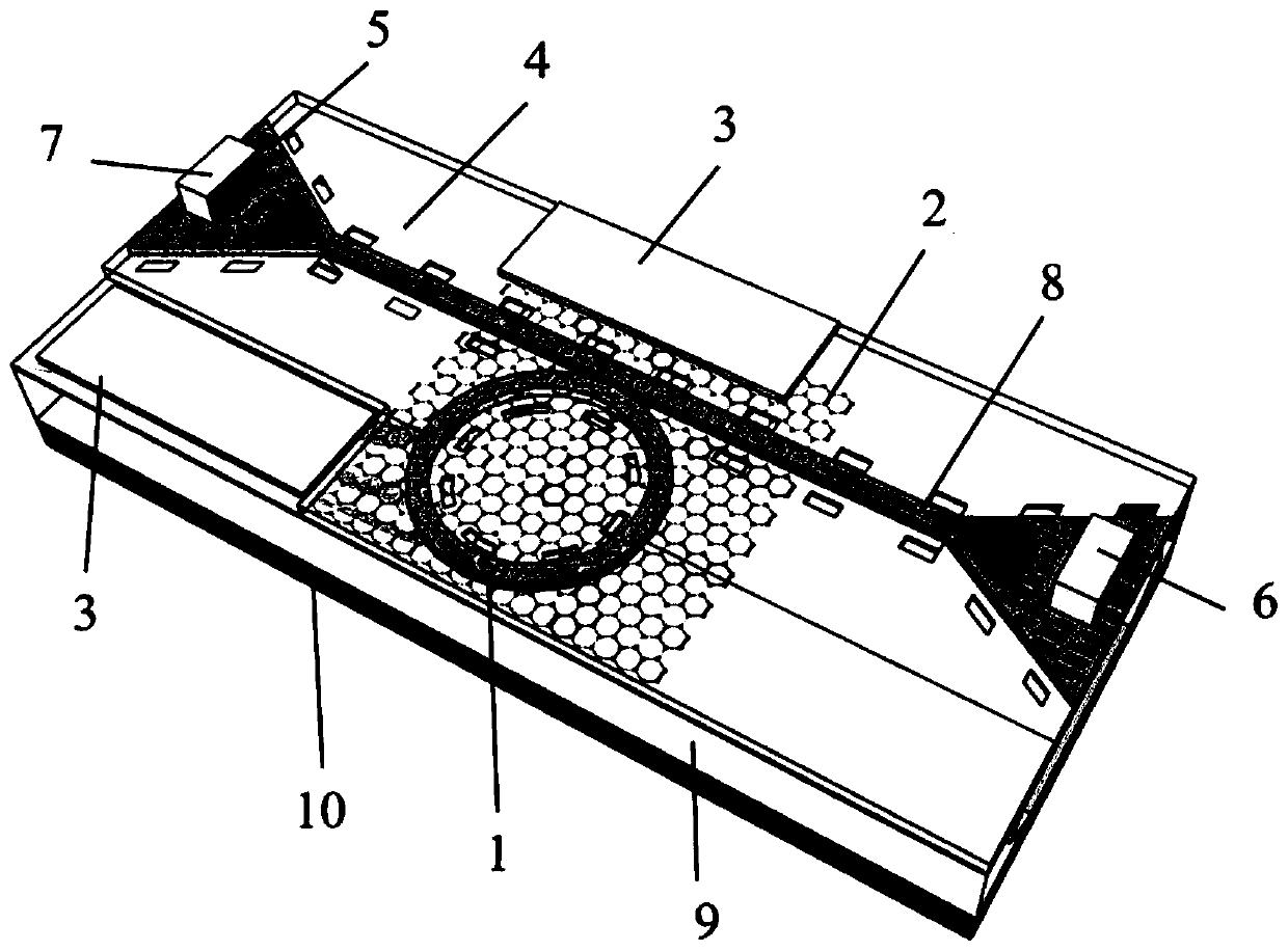
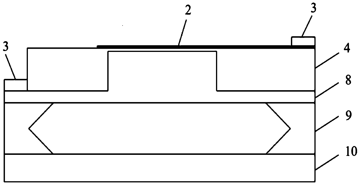
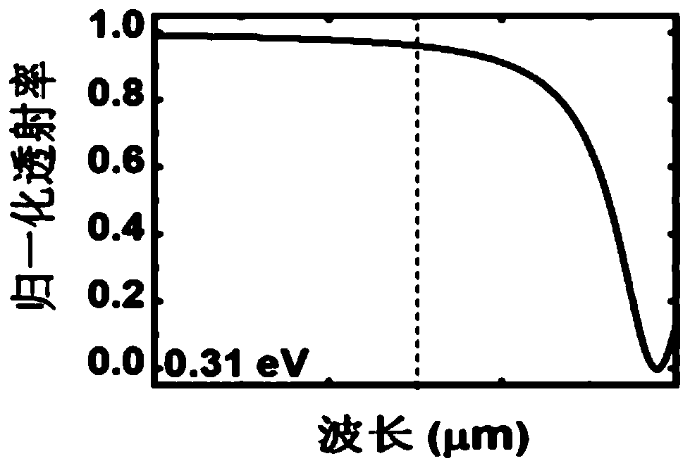
[0048] Such as figure 2 A graphene-silicon-based waveguide is shown, and its structural parameters are as follows: a silicon-on-insulator (SOI) wafer has a 340 nm thick top silicon layer and a 2 μm thick buried oxide layer, the waveguide is a ridge waveguide, and the waveguide width is 1 μm. The etching depth is 240nm, and the buried oxide layer at the lower part of the waveguide is etched away by hydrofluoric acid solution to reduce the absorption of mid-infrared light. According to theoretical calculations, the above-mentioned waveguide structure can support the propagation of the fundamental mode of mid-infrared light with a wavelength of 2.75 μm. In a specific embodiment, a microring resonator with a radius of 25 μm is used, the thickness of the aluminum oxide insulating cladding is 50 nm, and the coupling coefficient of the microring resonator is 0.98. Adjusting the Fermi levels of graphene to 0.31, 0.34, 0.37, 0.40, 0.43, 0.46, and 0.49eV respectively, the effective re...

Embodiment 2

[0052] Such as figure 2 A graphene-silicon-based waveguide is shown, and its structural parameters are as follows: a silicon-on-insulator (SOI) wafer has a 340 nm thick top silicon layer and a 2 μm thick buried oxide layer, the waveguide is a ridge waveguide, and the waveguide width is 1 μm. The etching depth is 240nm, and the buried oxide layer at the lower part of the waveguide is etched away by hydrofluoric acid solution to reduce the absorption of mid-infrared light. According to theoretical calculations, the above-mentioned waveguide structure can support the propagation of the fundamental mode of mid-infrared light with a wavelength of 2.75 μm. In a specific embodiment, a microring resonator with a radius of 25 μm is used, the thickness of the aluminum oxide insulating cladding is 50 nm, and the coupling coefficient of the microring resonator is 0.98. Adjusting the Fermi levels of graphene to 0.31, 0.34, 0.37, 0.40, 0.43, 0.46, and 0.49eV respectively, the effective re...


PUM

PropertyMeasurementUnit
radiusaaaaaaaaaa
thicknessaaaaaaaaaa

Abstract

The invention discloses a resonant cavity enhanced monolithic integrated sensor and a measurement method. The sensor comprises a resonant cavity, a two-dimensional material layer, electrodes, an insulating cladding, couplers, a monochromatic laser, a photoelectric detector, a waveguide, an insulating layer and a substrate layer; the insulating cladding and the two-dimensional material layer are sequentially located above the resonant cavity from bottom to top, the insulating layer and the substrate layer are sequentially located below the resonant cavity from top to bottom, and the waveguide and the resonant cavity are located on the same layer and located on one side of the resonant cavity; one electrode of the two electrodes is located on the waveguide, the other electrode is located onthe two-dimensional material layer, the couplers are arranged at the two ends of the waveguide, and the monochromatic laser and the photoelectric detector are connected with the couplers respectively.The sensor can be used for on-chip detection of waveguide environment refractive index change caused by biochemical molecules or on-chip detection of absorption spectra of the biochemical molecules.

Description

technical field [0001] The invention relates to the technical field of integrated optics, in particular to a resonant cavity-enhanced monolithic integrated sensor and a measurement method. Background technique [0002] Due to the advantages of CMOS-compatible fabrication process and low power consumption, graphene-silicon-based integrated optical circuits have received extensive attention in the past few years. On the one hand, the light propagating in the waveguide interacts with the graphene integrated on the surface of the waveguide through the evanescent field, which overcomes the weak absorption of vertically incident light by single-layer graphene. On the other hand, by changing the Fermi level of graphene by an external electric field, the intensity and phase of the propagating light in the waveguide can be adjusted to achieve light field modulation. Therefore, graphene-silicon integrated optical circuits are widely used to develop on-chip integrated electro-optic mo...

Claims


Application Information

Patent Timeline
Patent Type & Authority Applications(China)
IPC IPC(8): G01M11/02G01N21/31G01N21/41
CPCG01M11/0228G01N21/41G01N21/31
Inventor 程振洲陈威成韩森淼胡浩丰刘铁根
Owner TIANJIN UNIV
Why Eureka
Try Eureka