Preparation method of nanoring

A nano-ring and nano-scale technology, which is applied in the coupling of optical waveguides, the manufacture of microstructure devices, and the process for producing decorative surface effects. It can solve the problems of high cost, long time consumption, and difficulty in preparing nano-patterns on a large scale. , to achieve low-cost preparation and solve the effect of complex process

Active Publication Date: 2020-07-28
SOUTH UNIVERSITY OF SCIENCE AND TECHNOLOGY OF CHINA
View PDF6 Cites 2 Cited by
  • Summary
  • Abstract
  • Description
  • Claims
  • Application Information

AI Technical Summary

Problems solved by technology

But at the same time, its exposure method also determines that this process is time-consuming and costly, and it is difficult to prepare nano-patterns on a large scale on a wafer; The transfer of nanostructures to wafers has high resolution, but the initial imprint template needs to be prepared by e-book exposure or diffraction lithography, the cost is high, and the yield rate of nanoimprinting in the preparation of large-area micro-nano structures There is still room for improvement; microsphere mask etching is to lay nanometer microspheres with uniform particle size on the surface of the wafer, and use the microsphere mask to etch the wafer. In this process, microspheres are consumables, so the cost is high ; and it is difficult to achieve large-scale uniformity when transferring microspheres to the surface of the wafer

Method used


Image

  • Preparation method of nanoring
  • Preparation method of nanoring
  • Preparation method of nanoring

Examples


Embodiment 1

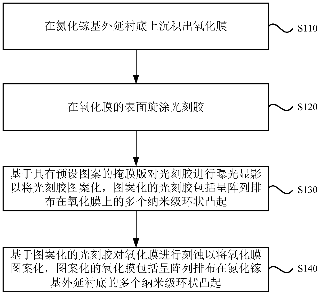
[0048] Such as figure 1 As shown, Embodiment 1 of the present invention provides a method for preparing a nanoring, the method comprising:

[0049] S110, depositing an oxide film on the GaN-based epitaxial substrate.

[0050] S120, spin-coating photoresist on the surface of the oxide film.

[0051] In this embodiment, when preparing gallium nitride-based nanorings, it is first necessary to deposit an oxide film on a gallium nitride-based epitaxial substrate, wherein the gallium nitride-based epitaxial substrate can be a gallium nitride-based LED wafer, consisting of The material of the epitaxial substrate can also include aluminum nitride, indium nitride or other ternary and quaternary alloy materials. Optionally, the plasma-enhanced chemical vapor phase epitaxy (PECVD) method is used to deposit on the gallium nitride-based LED wafer An oxide film is produced, wherein the oxide film can be a silicon dioxide film layer. After the oxide film is deposited, a photoresist needs t...

Embodiment 2

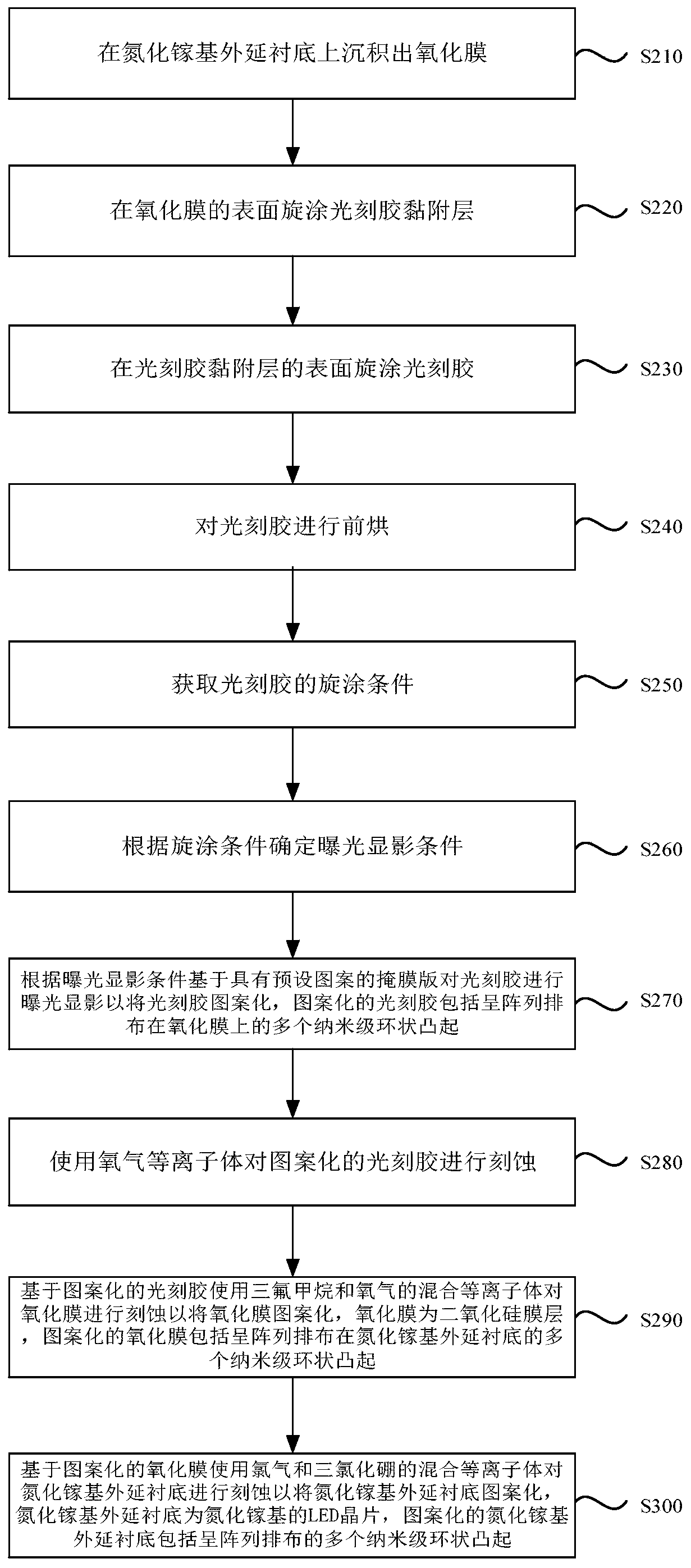
[0058] Such as figure 2 As shown, Embodiment 2 of the present invention provides a method for preparing nanorings. Embodiment 2 of the present invention is a further explanation on the basis of Embodiment 1 of the present invention. The method includes:

[0059] S210, depositing an oxide film on the GaN-based epitaxial substrate.

[0060] S220, spin coating a photoresist adhesion layer on the surface of the oxide film.

[0061] S230. Spin-coat photoresist on the surface of the photoresist adhesion layer.

[0062] S240, pre-baking the photoresist.

[0063] In this embodiment, before the photoresist is spin-coated on the surface of the oxide film, a photoresist adhesion layer needs to be spin-coated on the surface of the oxide film to increase the adhesion between the photoresist and the surface of the oxide film, and then the photoresist The surface of the adhesion layer is spin-coated with photoresist. After the photoresist is spin-coated, the photoresist needs to be pre-b...


PUM

PropertyMeasurementUnit
diameteraaaaaaaaaa

Abstract

The embodiment of the invention discloses a preparation method of a nanoring. The method comprises the following steps: depositing an oxide film on a gallium nitride-based epitaxial substrate; spin-coating photoresist on the surface of the oxide film; carrying out exposure and development on the photoresist based on a mask plate with a preset pattern so as to pattern the photoresist, wherein the patterned photoresist comprises a plurality of nanoscale annular bulges arranged on the oxide film in an array manner; and etching the oxide film based on the patterned photoresist so as to pattern theoxide film, wherein the patterned oxide film comprises a plurality of nanoscale annular bulges which are arranged on the gallium nitride-based epitaxial substrate in an array manner. The embodiment of the invention realizes simple and low-cost preparation of the GaN-based nanoring.

Description

technical field [0001] The embodiments of the present invention relate to semiconductor technology, and in particular to a method for preparing a nanoring. Background technique [0002] With the maturity of modern microfabrication technology, the third-generation semiconductor devices are advancing towards micro-nano-scale low-dimensional structures. At the micro-nano scale, the quantum confinement effect of semiconductor devices is becoming more and more obvious. Therefore, low-dimensional semiconductor devices based on micro-nano structures exhibit physical properties that are completely different from those of bulk materials in terms of optics and electricity, and have attracted much attention in the past decade. [0003] For the GaN-based light-emitting devices in the third-generation semiconductor devices, in the GaN-based nanoring structure, because the thickness of the ring wall is only a few hundred nanometers, the stress in the GaN-based material is released, which ...

Claims


Application Information

Patent Timeline
Patent Type & Authority Applications(China)
IPC IPC(8): B81B7/04B81C1/00
CPCB81B7/04B81C1/00031B81C1/00103Y02P70/50
Inventor 刘召军蒋府龙李四龙
Owner SOUTH UNIVERSITY OF SCIENCE AND TECHNOLOGY OF CHINA
Why Eureka
Try Eureka