Preparation method of gallium-doped polycrystalline silicon film, and application of gallium-doped polycrystalline silicon film in solar cells

A polysilicon thin film and thin film technology, applied in circuits, photovoltaic power generation, electrical components, etc., can solve the problems of reduced carrier lifetime, high diffusion rate, high Auger recombination, etc., and achieves reliable performance, large process window, repeatability strong effect

Pending Publication Date: 2020-08-07
NINGBO INST OF MATERIALS TECH & ENG CHINESE ACADEMY OF SCI
View PDF4 Cites 4 Cited by
  • Summary
  • Abstract
  • Description
  • Claims
  • Application Information

AI Technical Summary

Problems solved by technology

[0005] (2) Boron in SiO 2 layer has low diffusivity, and in SiO 2 It is easy to accumulate in the layer, making the overall passivation effect poor;
[0006] (3) The diffusion rate of boron in silicon is high, and it will quickly diffuse into the silicon wafer in large quantities under high-temperature annealing, thereby forming a higher Auger recombination and reducing the carrier lifetime;

Method used


Image

  • Preparation method of gallium-doped polycrystalline silicon film, and application of gallium-doped polycrystalline silicon film in solar cells
  • Preparation method of gallium-doped polycrystalline silicon film, and application of gallium-doped polycrystalline silicon film in solar cells
  • Preparation method of gallium-doped polycrystalline silicon film, and application of gallium-doped polycrystalline silicon film in solar cells

Examples


Embodiment 1

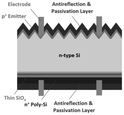
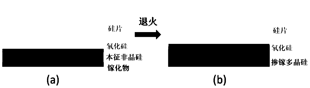
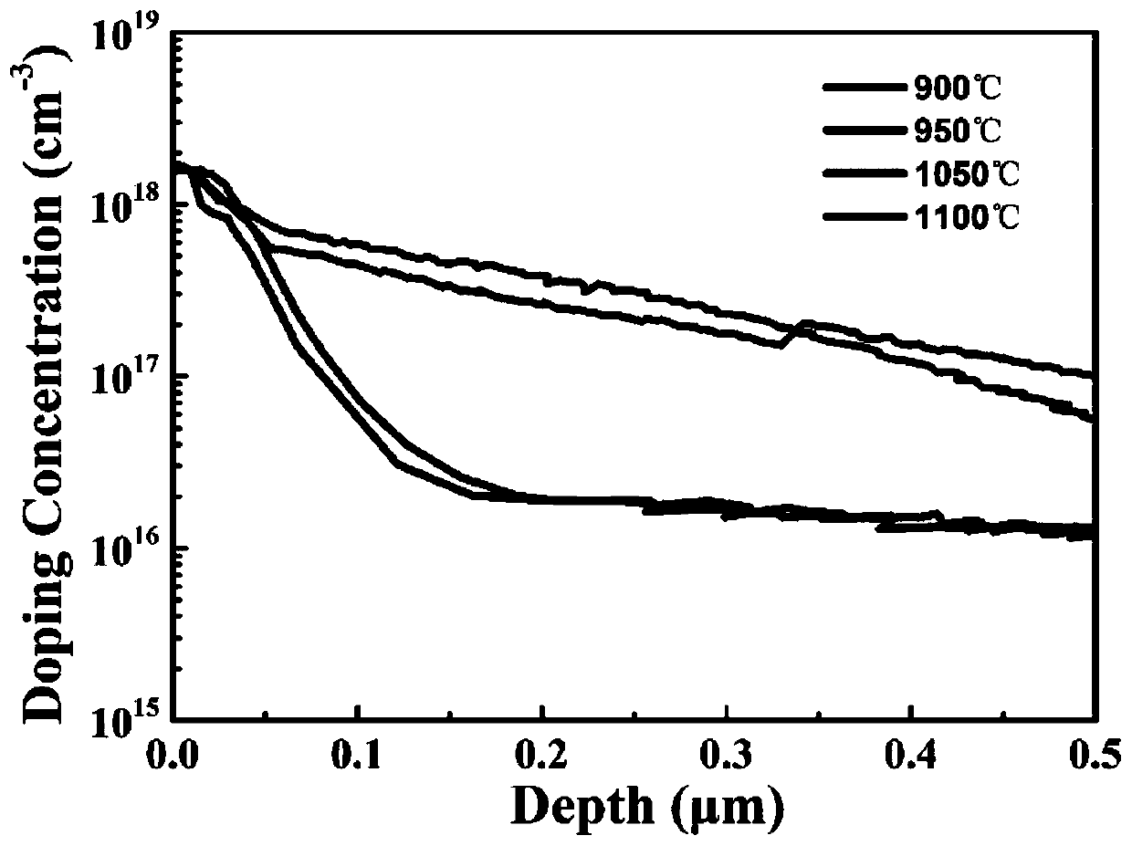
[0029] First, standard RCA cleaning is performed on the silicon wafer to ensure that the surface is sufficiently clean; then a high-quality silicon oxide tunneling layer is prepared on both sides by thermal nitric acid oxidation; an intrinsic amorphous silicon layer with a thickness of 40nm is deposited on both sides by PECVD; A 10nm GaO layer was deposited by electron beam evaporation; the sample was annealed at a high temperature of 1100°C for 60 minutes, the protective atmosphere was a mixture of nitrogen and hydrogen, and then the temperature began to drop; when the temperature dropped below 600°C, water vapor was introduced and kept warm. Using ECV to measure the diffusion curve, it can be seen that gallium atoms can be activated and diffused into the silicon wafer, thereby forming a field passivation effect; at the same time, we can see that gallium atoms do not form accumulations at the silicon oxide interface. Use Sinton WCT-120 to measure passivation quality, typical p...

Embodiment 2

[0031] First, standard RCA cleaning is performed on the silicon wafer to ensure that the surface is sufficiently clean; then a high-quality silicon oxide tunneling layer is prepared on both sides by thermal oxidation; an intrinsic amorphous silicon layer with a thickness of 40nm is deposited on both sides by PECVD; 10nm Ga(NO 3 ) 2 Layer; place the sample at 1050°C for high temperature annealing for 60 minutes, the protective atmosphere is a mixture of nitrogen and hydrogen, and then start to cool down; when the temperature drops below 600°C, pass in water vapor and keep it warm. Using ECV to measure the diffusion curve, it can be seen that the activation concentration of gallium atoms reaches 0-5*10 18 cm -3 , and diffused into the silicon wafer, can form a significant field passivation effect. Use Sinton WCT-120 to measure passivation quality, typical passivation quality iV oc Reach 710 ~ 720mV.

Embodiment 3

[0033] First, standard RCA cleaning is performed on the silicon wafer to ensure that the surface is sufficiently clean; then high-quality silicon oxide tunneling layer is prepared on both sides by plasma-assisted laughing gas oxidation; intrinsic amorphous silicon with a thickness of 40nm is deposited on both sides by PECVD layer; 10nm Ga 2 O layer; place the sample at 950°C for high temperature annealing for 60 minutes, the protective atmosphere is a mixture of nitrogen and hydrogen, and then start to cool down; when the temperature drops below 600°C, inject water vapor and keep it warm. Using ECV to measure the diffusion curve, it can be seen that the activation concentration of gallium atoms reaches 0-5*10 18 cm -3 , and diffused into the silicon wafer, can form a significant field passivation effect. Use Sinton WCT-120 to measure passivation quality, typical passivation quality iV oc Reach 710 ~ 720mV.


PUM

PropertyMeasurementUnit
thicknessaaaaaaaaaa
thicknessaaaaaaaaaa
thicknessaaaaaaaaaa

Abstract

The invention discloses a preparation method of a gallium-doped polycrystalline silicon film. The preparation method comprises the following steps: preparing a dielectric layer material on the surfaceof a cleaned silicon wafer; further depositing an intrinsic silicon film layer; then depositing a layer of a gallium-containing compound on the surface of the intrinsic silicon film by using a physical deposition method, wherein the intrinsic silicon layer and the gallium-containing compound can be repeatedly and alternately deposited; and carrying out high-temperature annealing at a temperatureof 800 DEG C or above in a protective atmosphere. According to the invention, the passivation quality of a p type silicon oxide / polycrystalline silicon passivation contact technology is effectively improved, and J0 and s can be reduced to below 10 fA / cm<2>; gallium source materials are rich and wide in source; the required equipment is simple, the treatment method is diversified, the repeatabilityis strong, and the process window is large; the p type silicon oxide / polycrystalline silicon passivation contact is simple in structure, reliable in performance and completely suitable for back passivation of a silicon oxide / polycrystalline silicon passivation contact battery; and the technical cost is relatively low, and the practicability is relatively high.

Description

technical field [0001] The invention relates to the field of solar cell components, in particular to the preparation of polysilicon thin films. Background technique [0002] The tunneling oxygen passivated emitter solar cell (TOPCon) is a new type of silicon solar cell proposed by the Fraunhofer Institute in Germany in 2013 (see the attached figure 1 ), is a battery device that achieves full-area high-efficiency passivation and carrier collection by silicon oxide and doped polysilicon. At present, it can be divided into two categories: p-type TOPCon (boron-doped polysilicon and silicon oxide layer) that collects holes and n-type TOPCon (phosphorus-doped polysilicon and silicon oxide layer) that collects electrons. On n-type silicon wafers, n-type TOPCon has an excellent passivation level, and the key indicator of passivation quality - single-sided saturated dark field current (J 0,s ) can easily achieve 10fA / cm 2 Below; while the passivation quality of p-type TOPCon is us...

Claims


Application Information

Patent Timeline
Patent Type & Authority Applications(China)
IPC IPC(8): H01L31/18H01L31/0216H01L31/068
CPCH01L31/182H01L31/02167H01L31/068Y02E10/546Y02P70/50
Inventor 黄丹丹叶继春曾俞衡闫宝杰廖明墩卢琳娜王志学郑晶茗
Owner NINGBO INST OF MATERIALS TECH & ENG CHINESE ACADEMY OF SCI
Why Eureka
Try Eureka