Graphene/monatomic layer GaS/GaAs radio generator and manufacturing method thereof

A single atomic layer, graphene layer technology, applied in circuits, electrical components, circuit devices, etc., can solve problems such as difficult preparation and large-scale integration

Active Publication Date: 2020-09-08
ZHEJIANG UNIV
View PDF5 Cites 1 Cited by
  • Summary
  • Abstract
  • Description
  • Claims
  • Application Information

AI Technical Summary

Problems solved by technology

However, the current research has not involved the graphene structure that collects and converts radio energy into electrical energy. Most of the research only involves the tunneling structure of metal-insulator-metal, but this structure is too difficult to prepare and integrate on a large scale. Inventing a simple The wireless charging device of the structure will provide convenient energy supply for the sensor devices and equipment of the Internet of Things

Method used


Image

  • Graphene/monatomic layer GaS/GaAs radio generator and manufacturing method thereof
  • Graphene/monatomic layer GaS/GaAs radio generator and manufacturing method thereof
  • Graphene/monatomic layer GaS/GaAs radio generator and manufacturing method thereof

Examples


Embodiment 1

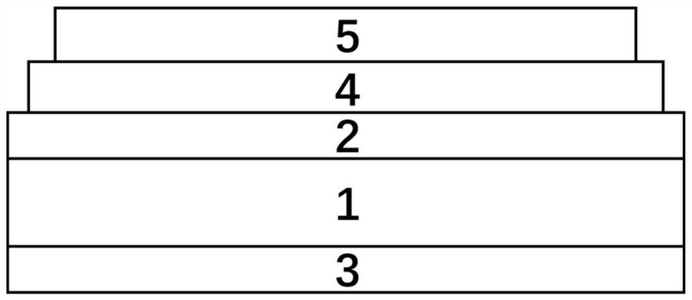
[0024] 1) After making the first electrode (titanium gold) on the back of GaAs, the GaAs wafers were cleaned as follows: first ultrasonically cleaned with acetone for 5 minutes, then cleaned with deionized water three times, and then with dilute hydrochloric acid solution to remove oxidation layer, then wash off the diluted hydrochloric acid, then oxidize the surface of GaAs with hydrogen peroxide solution, repeat the deoxidation and oxidation operation 3-7 times, passivate the GaAs sample with 18% ammonium sulfide solution, and finally use deionized water cleaning completed;

[0025] 2) Take a piece of copper-based graphene spin-coated with PMMA, and cut it into a regular shape of 0.5cm×0.5cm. Place the cut copper-based graphene on the upper surface of the copper foil etching solution. Transfer the etched graphene+PMMA layer to deionized water for cleaning with a glass slide, and transfer and clean for 3-5 times;

[0026] 3) Transfer the cleaned graphene to the front of gal...

Embodiment 2

[0029] 1) After the first electrode (Ti / Au) was fabricated on the back of GaAs, the GaAs wafers were cleaned as follows: first ultrasonically cleaned with acetone for 5 minutes, then cleaned with deionized water three times, and then removed with dilute hydrochloric acid solution. The oxide layer was washed off with dilute hydrochloric acid, and then the surface of GaAs was oxidized with hydrogen peroxide solution. After repeating the deoxidation and oxidation operations for 3-7 times, the GaAs sample was passivated with 12% ammonium sulfide solution for 15 minutes. Deionized water cleaning is completed;

[0030] 2) Take a piece of copper-based graphene spin-coated with PMMA, and cut it into a regular shape of 0.5cm×0.5cm. Place the cut copper-based graphene in the copper foil etching solution (the graphene side faces up). Transfer the etched graphene+PMMA layer to deionized water for cleaning with a glass slide, and transfer and clean for 3-5 times;

[0031] 3) Transfer the...

Embodiment 3

[0034] 1) After the first electrode (Ti / Au) was fabricated on the back of GaAs, the GaAs wafers were cleaned as follows: first ultrasonically cleaned with acetone for 5 minutes, then cleaned with deionized water three times, and then removed with dilute hydrochloric acid solution. The oxide layer was washed off with dilute hydrochloric acid and then oxidized the surface of GaAs with hydrogen peroxide solution. Repeat the deoxidation and oxidation operations for 3-7 times, then passivate the GaAs sample with 18% ammonium sulfide solution for 30 minutes, and finally use deionized water cleaning completed;

[0035] 2) Take a piece of copper-based graphene spin-coated with PMMA, and cut it into a regular shape of 0.5cm×0.5cm. Place the cut copper-based graphene in the copper foil etching solution (the graphene side faces up). Transfer the etched graphene+PMMA layer to deionized water for cleaning with a glass slide, and transfer and clean for 3-5 times;

[0036] 3) Transfer the ...


PUM

PropertyMeasurementUnit
thicknessaaaaaaaaaa

Abstract

The invention relates to a radio power generation device and discloses a graphene/monatomic layer GaS/gallium arsenide radio generator. A layer of monatomic layer GaS is formed on a gallium arsenide substrate passivated by ammonium sulfide, a layer of graphene is attached to the layer of monatomic layer GaS, a first electrode and a side electrode are arranged, and the graphene is in direct contactwith a monatomic layer gallium sulfide surface of gallium arsenide to form a heterojunction. The key point of the generator lies in that graphene contacts gallium arsenide passivated by ammonium sulfide to form a Schottky junction and a Schottky barrier, t radio frequency waves (sub-6G) emitted by an emission source can be collected, the quantum property of the radio frequency waves stimulates hot electrons in the graphene, and a tunneling process occurs to form a current. External radio frequency waves are directly converted into direct-current electric energy, and electric energy can be provided for electronic equipment such as wearable equipment and sensors anytime and anywhere. Compared with traditional wireless charging equipment, the generator is more flexible, higher in efficiencyand simple in device structure.

Description

technical field [0001] The invention relates to a radio generator and a preparation method thereof, in particular to a graphene / single atomic layer GaS / gallium arsenide generator and a preparation method thereof, belonging to the fields of wireless energy and wireless sensing. Background technique [0002] With the emerging development in the fields of artificial intelligence, drones, wearable devices, and the popularity of the Internet of Things, wireless charging devices that can obtain in-situ energy anytime, anywhere have gained widespread attention. The use of wireless charging to charge the battery is beneficial to the long-term operation of the battery and saves a lot of battery maintenance and replacement work. Wireless energy transmission technology has the advantages of flexibility, convenience, safety and reliability, non-contact power supply, easy control and less external influence. Obtaining energy from radio waves has great development prospects in the future,...

Claims


Application Information

Patent Timeline
Patent Type & Authority Applications(China)
IPC IPC(8): H02J50/20H01L31/115H01L31/0336
CPCH02J50/20H01L31/115H01L31/0336
Inventor 林时胜宣扬帆陈红陈妍郑浩男陆阳华
Owner ZHEJIANG UNIV
Why Eureka
Try Eureka