Silicon-based heterojunction solar cell and preparation method thereof

A solar cell and heterojunction technology, applied in circuits, photovoltaic power generation, electrical components, etc., can solve problems such as small variable range of work function, achieve the effects of increasing short-circuit current density, improving conversion efficiency, and low process temperature

Pending Publication Date: 2020-09-11
晋能光伏技术有限责任公司
View PDF0 Cites 11 Cited by
  • Summary
  • Abstract
  • Description
  • Claims
  • Application Information

AI Technical Summary

Problems solved by technology

[0005] Microcrystalline silicon thin films, microcrystalline silicon silicon oxygen thin films, and microcrystalline silicon carbon thin films have become research hotspots in recent years due to their advantages of wide band gap and weak light absorption. These materials also need to match TCO thin films with different work functions. As far as the TCO material (or target material) is concerned, the work function is basically fixed. In the existing reports, it can be slightly adjusted by adjusting the oxygen flux of the process, the pressure or power of deposition and film formation, but generally speaking, its work function The variable range is small

Method used


Image

  • Silicon-based heterojunction solar cell and preparation method thereof
  • Silicon-based heterojunction solar cell and preparation method thereof
  • Silicon-based heterojunction solar cell and preparation method thereof

Examples


Embodiment 1

[0049] A method for preparing a silicon-based heterojunction solar cell, specifically comprising the following steps:

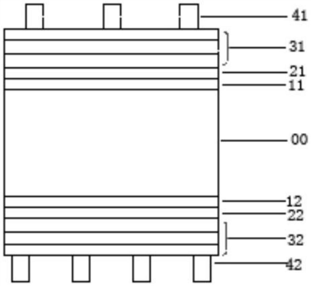
[0050] (1) Texturing and cleaning the crystalline silicon wafer to obtain the crystalline silicon substrate 00;

[0051] (2) Utilizing plasma chemical vapor deposition, depositing the first intrinsic amorphous silicon layer 11 and the first doped layer 21 sequentially on the upper surface of the crystalline silicon substrate 00, and depositing the first intrinsic amorphous silicon layer 21 sequentially on the lower surface of the crystalline silicon substrate 00. Two intrinsic amorphous silicon layers 12 and a second doped layer 22;

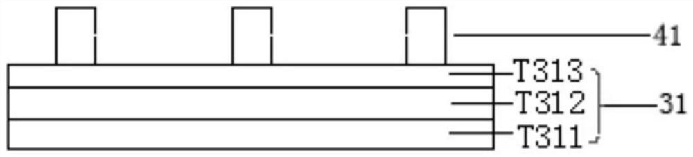
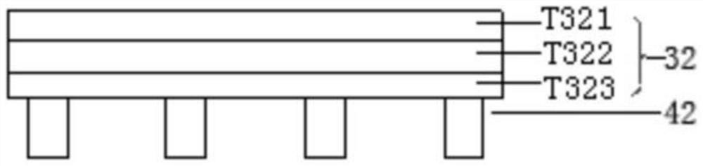
[0052] (4) Utilize the magnetron sputtering mode, deposit the first TCO film 311, the second TCO film 312 and the 3rd TCO film 313 successively on the upper surface of the first doped layer 21, meanwhile, process and first doped layer 21 (n-type amorphous silicon) contact with the first TCO film 311, use plasma chemical vapor d...

Embodiment 2

[0056] A method for preparing a silicon-based heterojunction solar cell, specifically comprising the following steps:

[0057] (1) Texturing and cleaning the crystalline silicon wafer to obtain the crystalline silicon substrate 00;

[0058] (2) Utilizing plasma chemical vapor deposition, depositing the first intrinsic amorphous silicon layer 11 and the first doped layer 21 sequentially on the upper surface of the crystalline silicon substrate 00, and depositing the first intrinsic amorphous silicon layer 21 sequentially on the lower surface of the crystalline silicon substrate 00. Two intrinsic amorphous silicon layers 12 and a second doped layer 22;

[0059] (4) Utilize the electron beam evaporation mode, deposit the first TCO thin film 311, the second TCO thin film 312 and the third TCO thin film 313 successively on the upper surface of the first doped layer 21, meanwhile, process and first doped layer 21 (n-type amorphous silicon) contact with the first TCO thin film 311, ...

Embodiment 3

[0063] A method for preparing a silicon-based heterojunction solar cell, specifically comprising the following steps:

[0064] (1) Texturing and cleaning the crystalline silicon wafer to obtain the crystalline silicon substrate 00;

[0065] (2) Utilizing plasma chemical vapor deposition, depositing the first intrinsic amorphous silicon layer 11 and the first doped layer 21 sequentially on the upper surface of the crystalline silicon substrate 00, and depositing the first intrinsic amorphous silicon layer 21 sequentially on the lower surface of the crystalline silicon substrate 00. Two intrinsic amorphous silicon layers 12 and a second doped layer 22;

[0066] (4) Utilize the reactive plasma deposition method, deposit the first TCO thin film 311, the second TCO thin film 312 and the third TCO thin film 313 successively on the upper surface of the first doped layer 21, meanwhile, process and first doped layer 21 (n-type amorphous silicon) contact with the first TCO film 311, use ...


PUM

PropertyMeasurementUnit
thicknessaaaaaaaaaa
thicknessaaaaaaaaaa
thicknessaaaaaaaaaa

Abstract

The invention discloses a silicon-based heterojunction solar cell. The silicon-based heterojunction solar cell comprises a crystalline silicon substrate; a first intrinsic amorphous silicon layer, a first doping layer, a first TCO layer and a first metal electrode are sequentially arranged on the upper surface of the crystalline silicon substrate; a second intrinsic amorphous silicon layer, a second doping layer, a second TCO layer and a second metal electrode are sequentially arranged on the lower surface of the crystalline silicon substrate. The preparation method comprises the following steps: (1), obtaining a crystalline silicon substrate; (2), carrying out plasma chemical vapor deposition on a first intrinsic amorphous silicon layer, a second intrinsic amorphous silicon layer, a firstdoping layer and a second doping layer ; (4), depositing a first TCO layer and a second TCO layer, and performing plasma treatment at the same time; and (5), forming a first metal electrode and a second metal electrode through silk-screen printing. The method is rapid, practical and easy to implement, the functional interface contact of TCO and doped amorphous silicon can be optimized, and the conversion efficiency of the heterojunction solar cell is remarkably improved.

Description

technical field [0001] The invention relates to the technical field of solar cell manufacturing, and more specifically relates to a silicon-based heterojunction solar cell and a preparation method thereof. Background technique [0002] Silicon-based heterojunction solar cell (HJT, heterojunction solar cell with intrinsicthin layer) has a symmetrical structure, which not only provides good surface passivation, but also has a process temperature lower than 250°C and a simple preparation process, because of its ultra-high conversion efficiency and attention to development potential. The main process steps involved in HJT solar cells are: depositing intrinsic amorphous silicon with nanoscale thickness on both sides of the textured crystalline silicon substrate, depositing doped amorphous silicon or microcrystalline silicon on the intrinsic amorphous silicon layer. For the crystalline silicon layer, in order to effectively export electrons, it is necessary to prepare transparent...

Claims


Application Information

Patent Timeline
Patent Type & Authority Applications(China)
IPC IPC(8): H01L31/075H01L31/076H01L31/0216H01L31/18
CPCH01L31/02167H01L31/075H01L31/076H01L31/18Y02E10/548Y02P70/50
Inventor 王继磊鲍少娟贾慧君白焱辉杨骥冯乐黄金张娟高勇
Owner 晋能光伏技术有限责任公司
Why Eureka
Try Eureka