Method for manufacturing high-precision fine lines on high-flatness surface of LTCC substrate

A production method and high-precision technology, applied in the fields of printed circuit manufacturing, cleaning/polishing of conductive patterns, secondary treatment of printed circuits, etc., can solve the problems of low adaptability of high-frequency LTCC materials, wire defects, and low yield. Achieve the effect of mature equipment and technology, high surface smoothness and small line fineness

Active Publication Date: 2020-09-18
SOUTHWEST CHINA RES INST OF ELECTRONICS EQUIP
View PDF7 Cites 0 Cited by
  • Summary
  • Abstract
  • Description
  • Claims
  • Application Information

AI Technical Summary

Problems solved by technology

However, the conventional LTCC is realized by co-firing. The conventional wiring fineness is 100 μm ± 10 μm, and the graphic position error caused by the substrate shrinkage deviation can reach ± ​​0.1 mm (calculated based on the substrate length of 35 mm and the sintering shrinkage deviation ± 0.3%). up to 0.1mm (caused by the stacking of the inner conductor film layer, substrate warping, etc.), which cannot meet the requirements of high-density chips for wiring fineness, position accuracy, and surface flatness (most high-density, multi-functional chips require substrate wiring fineness Reaching 50μm, the pattern position error is better than ±0.02mm, and the substrate surface flatness is better than 0.02mm, in order to achieve good undercut assembly)
[0004] In view of the demand for high-level and high-precision wiring on the LTCC substrate surface, there are two common methods in the industry. One is to use a high-precision screen to perform secondary wiring on the surface of the LTCC substrate after sintering through post-firing. This method can be effective. Eliminate the graphic position error caused by the shrinkage deviation of the substrate itself, but the fineness and precision of the printing screen are high, and the electronic paste is required to have very good printing resolution, so the application is relatively limited. Even so, the fineness of 50 μm can be achieved The difficulty of wiring is still huge, and the yield rate is low. The patents "LTCC substrate three-dimensional stacking structure and its hermetic packaging method" and "a BGA interconnection structure of LTCC substrate and its realization method" both use post-firing to make graphics. To eliminate the pattern position deviation caused by co-firing shrinkage deviation, but it is extremely difficult to achieve high-quality lines with a fineness of 50 μm
Another method is to use the thin film circuit preparation process, which is realized on the surface of the LTCC substrate after sintering by sputtering, photolithography, electroplating / electroless plating, but this method has a long process flow, high process cost, and requires the substrate surface and Dense, otherwise it is extremely easy to cause wire defects during the process, resulting in short wires or metallized particles between wire seams, resulting in short circuits
[0005] In recent years, with the development of laser technology, LDS technology has been widely used for circuit wiring on the surface of substrates or structural parts. Composite components and manufacturing methods of plastic raw materials", "Laser direct writing film and laser direct writing micro-nano pattern method", "Three-dimensional packaging structure and its manufacturing method", "Stacked package directly structured by laser", "A method for making a cathode for micro-electrolytic processing of surface texture", "An LDS electroless plating process", "LDS film antenna and its manufacturing method", "Connection method of three-dimensional circuit and metal parts and LDS antenna", " An LDS Antenna Structure for Electronic Products” all announced the use of LDS technology to make precise patterns on the surface of substrates or structural parts, but this method requires materials to be added with elements that can be activated by lasers, and has strong selectivity for materials. Many high-frequency LTCC materials have low adaptability

Method used


Image

  • Method for manufacturing high-precision fine lines on high-flatness surface of LTCC substrate
  • Method for manufacturing high-precision fine lines on high-flatness surface of LTCC substrate
  • Method for manufacturing high-precision fine lines on high-flatness surface of LTCC substrate

Examples


Embodiment Construction

[0028] The present invention will be further described below in conjunction with the accompanying drawings.

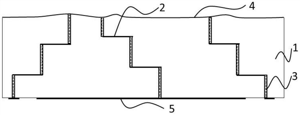
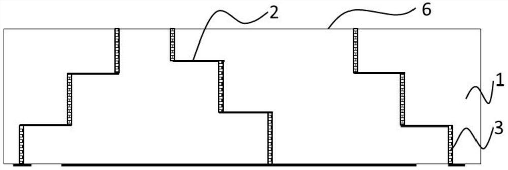
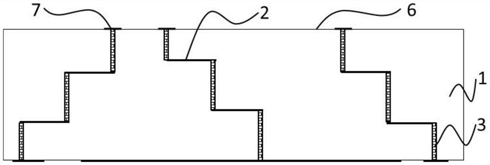
[0029] The present invention relates to the processing of LTCC circuit substrates, especially to make high-precision fine lines on the high flat surface of LTCC substrates to obtain high surface flatness, line fineness and line precision, so as to meet the requirements of high-density chip reverse assembly, support Fabrication of SIP high-density multi-function package.

[0030] The surface of the LTCC multi-layer circuit substrate is high-flat by grinding, the surface is made of high-precision fine lines by laser etching, and the slag on the edge of the conductor pattern is cleaned by high-temperature post-processing. The specific production process is as follows:

[0031] A method for manufacturing high-precision fine lines on a high-level surface of an LTCC substrate, comprising the following processes:

[0032] Step 1, smoothing the surface of the sintered multila...


PUM

PropertyMeasurementUnit
thicknessaaaaaaaaaa
thicknessaaaaaaaaaa
widthaaaaaaaaaa

Abstract

The invention relates to a method for manufacturing high-precision fine lines on a high-flatness surface of an LTCC substrate. The method comprises the following steps: 1, smoothing the surface of a sintered multilayer LTCC circuit substrate; 2, manufacturing a conductor pattern on the surface of the ground substrate; 3, precisely modifying the conductor pattern to obtain high-precision fine lines; 4, carrying out post-treatment on the precisely modified substrate to eliminate edge slag of the high-precision fine lines. By adopting the method to manufacture the LTCC surface high-precision finelines, high surface flatness can be obtained, conductor pattern arrangement is flexible, line fineness is small, precision is high, edges are smooth, the method has high compatibility with a materialsystem, and required equipment and processes are mature.

Description

technical field [0001] The invention relates to the field of circuit substrate processing, in particular to a method for manufacturing high-precision fine lines on the high-level surface of an LTCC substrate. Background technique [0002] With the further improvement of information equipment system for miniaturization, light weight, high density, and high performance, the assembly method of chip front mounting combined with gold wire / gold ribbon bonding in traditional multi-functional components can no longer meet the requirements for high integration density. , Low parasitic assembly requirements, so there is an urgent need for high-density, high-performance, multi-functional chips and functional substrates for reverse assembly. [0003] With its excellent high-frequency performance, high integration density and high reliability, LTCC technology has been widely used in aviation, aerospace, missile-borne, communication and other fields. However, the conventional LTCC is rea...

Claims


Application Information

Patent Timeline
Patent Type & Authority Applications(China)
IPC IPC(8): H05K3/00H05K3/02H05K3/26
CPCH05K3/0044H05K3/027H05K3/26H05K2203/107H05K2203/1105
Inventor 杨宇岳帅旗束平徐洋黄翠英张刚
Owner SOUTHWEST CHINA RES INST OF ELECTRONICS EQUIP
Why Eureka
Try Eureka