Amorphous Ga2O3 photoelectric detector and preparation method and performance improvement method thereof
A photodetector and amorphous technology, which is applied in the field of photoelectric detection, can solve the problems affecting the application effect of devices and the reduction of device responsivity, and achieve the effects of dark current reduction, dark current suppression, and light-to-dark ratio improvement
- Summary
- Abstract
- Description
- Claims
- Application Information
AI Technical Summary
Problems solved by technology
Method used
Image
Examples
preparation example Construction
[0043] Correspondingly, the embodiment of the present invention provides amorphous Ga 2 o 3 The preparation method of photodetector, its main flow can comprise:
[0044] Pretreatment of the substrate: The substrate is ultrasonically cleaned with chemical reagents and then blown dry.
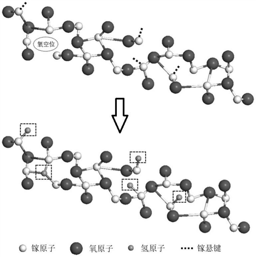
[0045] Put the pretreated substrate into the cavity of the vacuum deposition equipment, start the vacuum pump, and prepare hydrogen-doped amorphous Ga by vacuum deposition method in a hydrogen-containing atmosphere at 20°C to 400°C. 2 o 3 Thin-film active layer: Specifically, after starting the vacuum pump and pumping the cavity of the vacuum deposition equipment to the background vacuum, a high-precision gas flowmeter is used to feed hydrogen-containing gas, and record the amount of hydrogen-containing gas in the cavity Vacuum value, wait for a period of time after the flow rate of the hydrogen-containing gas and the vacuum in the cavity are stable, so that the hydrogen-containing gas is even...
Embodiment 1
[0056] This embodiment provides a high light-to-dark ratio amorphous Ga 2 o 3 A method for preparing a photodetector, the structure of which is a metal-semiconductor-metal (MSM) structure. The specific preparation method of the photodetector of the present embodiment is as follows:
[0057] Step 1: Clean a piece of far-ultraviolet ultra-pure quartz substrate with a size of 15mm×15mm×0.5mm ultrasonically, blow it dry with dry high-purity nitrogen, and place it on a sample holder of the same size. After fixing the substrate, put it into the growth chamber of the magnetron sputtering instrument equipped with a gallium oxide ceramic target (the purity of the gallium oxide ceramic target used in this example is 99.999%), and the sample stage is raised to the highest point (target material The distance from the substrate is about 8mm), close the baffle under the sample, and finally tighten the quick release port of the chamber.
[0058] Step 2: Start the vacuum pumping system of ...
Embodiment 2
[0065] This embodiment is basically the same as Embodiment 1, the difference is that in step 2, after the background vacuum is lowered to less than 4.5E-4Pa, 1.0 sccm of high-purity hydrogen is introduced, and after the gas flow is stable, wait for 10 minutes. And the vacuum in the cavity has been stable, then 10sccm of high-purity argon gas is introduced, the vacuum in the cavity reaches 1.6E-1Pa, and the glow sputters Ga 2 o 3 Thin film, the film thickness is about 84nm. The resulting amorphous Ga 2 o 3 The photodetector is designated as sample 2.
PUM
| Property | Measurement | Unit |
|---|---|---|
| thickness | aaaaa | aaaaa |
| thickness | aaaaa | aaaaa |
| thickness | aaaaa | aaaaa |
Abstract
Description
Claims
Application Information


