

Piezoresistor adopting silicon rubber insulating layer, and manufacturing method thereof
A silicon rubber insulating layer and varistor technology, applied in varistors, overvoltage protection resistors, resistors, etc., can solve the problems of poor resistance to high and low temperature impact, achieve long service life, avoid dust pollution, Improve the effect of withstanding high current impact
- Summary
- Abstract
- Description
- Claims
- Application Information
AI Technical Summary
Problems solved by technology
Method used
Image

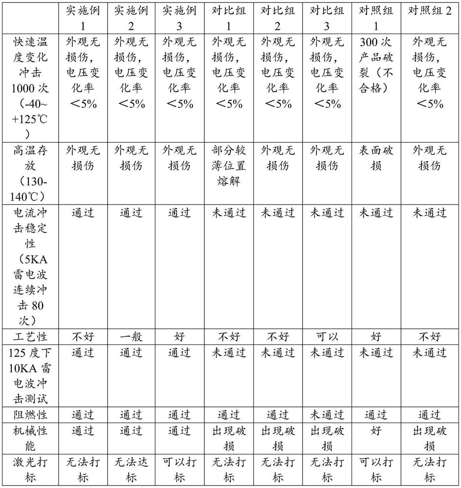
Examples
Embodiment 1
[0036] This embodiment specifically discloses a formula of insulating silicone rubber, which is an insulating material specially used for piezoresistors.
[0037] Since the varistor is mainly composed of a pressure-sensitive ceramic chip, pins and packaging layer, and the main function of the packaging layer is to isolate it from the external environment, to prevent moisture, dust particles and other pollutants from contaminating the chip, while the packaging layer It has extremely high insulation ability and adhesive force, and can avoid serious damage to ceramic chips caused by arc flashover when the voltage is too high.
[0038]The encapsulation layer in the prior art is a multi-material wrapping structure, because the role of the encapsulation layer is particularly important, especially in the case of high and low temperature cycle shocks, the stress caused by the different thermal expansion coefficients of various materials will directly act on the encapsulation layer, if ...
Embodiment 2
[0054] In this embodiment, a varistor is provided, which includes a cylindrical varistor ceramic body and pins arranged on the circular surfaces at both ends of the varistor ceramic body, and is wrapped with a soft silicone rubber layer for For sealing and insulation.
[0055] The soft silicone rubber layer is adjusted by a special formula, so that it has better high and low temperature impact resistance. The specific formula is as follows:
[0056] Hexamethyldisiloxane 5%
[0057] Ethyl orthosilicate 3%
[0058] Ethyl polysilicate 2%
[0059] Phenyl Silica Gel························· 25%
[0060] Hydroxy silicone oil 30%
[0061] Nitrogen Flame Retardant······························ 10%
[0062] Phosphorus Flame Retardant······························ 10%
[0063] Thixotropic agent······························ 10%
[0064] Curing agent 5%
[0065] Among them, the resin product is obtained by kneading the hexamethyldisiloxane, tetraethyl orthosilicate and polyethyl ...
Embodiment 3
[0068] In this embodiment, a varistor is provided, which includes a cylindrical varistor ceramic body and pins arranged on the circular surfaces at both ends of the varistor ceramic body, and is wrapped with a soft silicone rubber layer for For sealing and insulation.
[0069] The soft silicone rubber layer is adjusted by a special formula, so that it has better high and low temperature impact resistance. The specific formula is as follows:
[0070] Hexamethyldisiloxane···························· 5%
[0071] Ethyl orthosilicate 3%
[0072] Polyethylsilicate····························· 2%
[0073] Phenyl Silica Gel······························ 25%
[0074] Hydroxy silicone oil 30%
[0075] Nitrogen Flame Retardant··························· 10%
[0076] Phosphorus Flame Retardant··························· 10%
[0077] Thixotropic agent······························· 10%
[0078] Curing agent····························· 3%
[0079] Photosensitive color powder (titan...
PUM
 Abstract
Description
Claims
Application Information