Short-wavelength deep ultraviolet LED epitaxial structure and P-type layer material, preparation method and application thereof
A technology of epitaxial structure and layer materials, applied in electrical components, nanotechnology, circuits, etc., can solve the problem of restricting the luminous efficiency and application prospects of deep ultraviolet LEDs, restricting the luminous efficiency of short-wavelength deep ultraviolet LED devices, and deteriorating p-AlGaN thin film materials Crystal quality and other issues, to achieve the effect of improving current congestion, improving activation efficiency, and uniform distribution of lateral current
- Summary
- Abstract
- Description
- Claims
- Application Information
AI Technical Summary
Problems solved by technology
Method used
Image
Examples
Embodiment 1
[0032] Example 1: 355nm UV LED structure
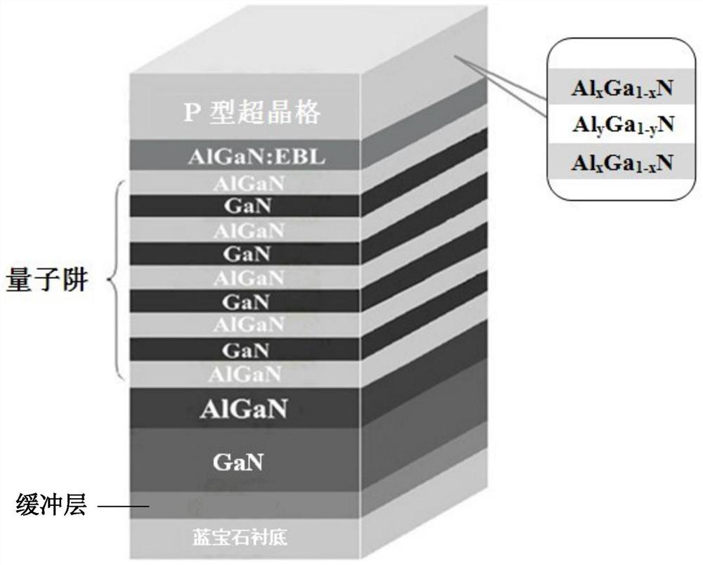
[0033] Step 1: First, set the pressure of the reaction chamber of the MOCVD system to 400mbar, at H 2 The c-plane sapphire substrate was baked at a high temperature at 1100°C and then cooled to 520°C to grow a 25nm thick GaN buffer nucleation layer, then raised to 1080°C for annealing and recrystallization, and then raised to 1140°C to grow a 2μm GaN support layer.
[0034] Step 2: Reduce the pressure in the reaction chamber to 80mbar and grow 550nm n-AlGaN, where the flow rates of TMGa and TMAl are set to 110 and 131μmol / min, respectively, and the effective Si doping concentration is 6sccm. Then turn off the Si doping source and continue to grow 50nm non- AlGaN is deliberately doped.
[0035] Step 3: Raise temperature to 1150℃ to grow GaN / Al for 5 cycles 0.1 Ga 0.9 N multiple quantum well structure, in which the GaN potential well layer TMGa flow rate is set to 110μmol / min, the Si effective doping concentration is 0.5sccm; the AlGaN barrier...
Embodiment 2
[0039] Embodiment 2: 310nm ultraviolet LED structure
[0040] Step 1: First set the pressure in the reaction chamber of the MOCVD system to 400mbar, bake the c-plane sapphire substrate at a high temperature of 1100°C in an H2 environment, then cool to 520°C to grow a 25nm thick GaN buffer nucleation layer, and then heat to 1080°C. Annealing is recrystallized, and then the temperature is raised to 1140°C to grow a 2μm GaN support layer.
[0041] Step 2: The reaction chamber is heated to 1160°C, the pressure is reduced to 80mbar, and a 550nm AlGaN insertion layer is grown. The flow rates of TMGa and TMAl are set to 110 and 392μmol / min, respectively. 3 The flow rate is 8000 sccm, the effective Si doping concentration is 6 sccm, and then the Si doping source is turned off, and the unintentionally doped AlGaN is grown by 50 nm.
[0042] Step 3: Increase the temperature to 1165℃ and grow Al for 5 cycles 0.1 Ga 0.9 N / Al 0.15 Ga 0.85 N multiple quantum well structure. Among them, Al 0.1 Ga ...
Embodiment 3
[0046] Embodiment 3: 280nm ultraviolet LED structure
[0047] Step 1: First, set the pressure of the reaction chamber of the MOCVD system to 400mbar, at H 2 The c-plane sapphire substrate was baked at a high temperature at 1100°C and then cooled to 520°C to grow a 25nm thick GaN buffer nucleation layer, then raised to 1080°C for annealing and recrystallization, and then raised to 1140°C to grow a 2μm GaN support layer.
[0048] Step 2: The pressure in the reaction chamber is reduced to 80mbar, and a 550nm AlGaN insertion layer is grown. The flow rates of TMGa and TMAl are set to 66 and 269μmol / min, respectively. 3 The flow rate is 8000 sccm, the effective Si doping concentration is 6 sccm, and then the Si doping source is turned off, and the unintentionally doped AlGaN of 50 nm is continued to grow.
[0049] Step 3: Increase the temperature to 1150℃ to grow Al for 5 cycles 0.3 Ga 0.7 N / Al 0.4 Ga 0.6 N multiple quantum well structure, Al 0.3 Ga 0.7 The flow rates of the N well layer TM...
PUM
| Property | Measurement | Unit |
|---|---|---|
| thickness | aaaaa | aaaaa |
Abstract
Description
Claims
Application Information
 - Generate Ideas
- Intellectual Property
- Life Sciences
- Materials
- Tech Scout
- Unparalleled Data Quality
- Higher Quality Content
- 60% Fewer Hallucinations
Browse by: Latest US Patents, China's latest patents, Technical Efficacy Thesaurus, Application Domain, Technology Topic, Popular Technical Reports.
© 2025 PatSnap. All rights reserved.Legal|Privacy policy|Modern Slavery Act Transparency Statement|Sitemap|About US| Contact US: help@patsnap.com


