Resonant acceleration sensor based on nano piezoelectric beam and preparation method of resonant acceleration sensor
A technology of acceleration sensor and piezoelectric beam, which is applied in the direction of measuring acceleration, speed/acceleration/shock measurement, instruments, etc., and can solve problems such as poor anti-overload ability, low resonance frequency, and low sensitivity
- Summary
- Abstract
- Description
- Claims
- Application Information
AI Technical Summary
Problems solved by technology
Method used
Image
Examples
Embodiment 1
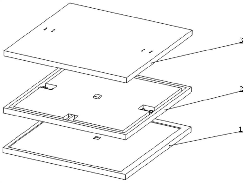
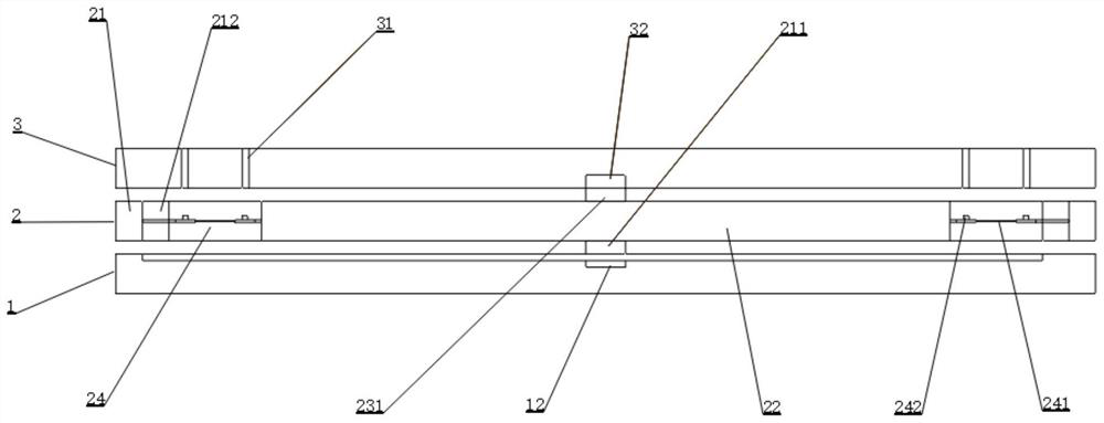
[0054] Such as Figure 1~4 As shown, the resonant acceleration sensor based on nano piezoelectric beams includes a substrate 1, a detection structure layer 2 and a cover plate 3;
[0055] The base 1 is made on the basis of a crystal orientation N-type single-polished silicon wafer. The top surface of the base 1 is a polished surface, and a movable cavity groove 11 is provided, and the center of the movable cavity groove 11 is provided with a lower limit position. slot 12;
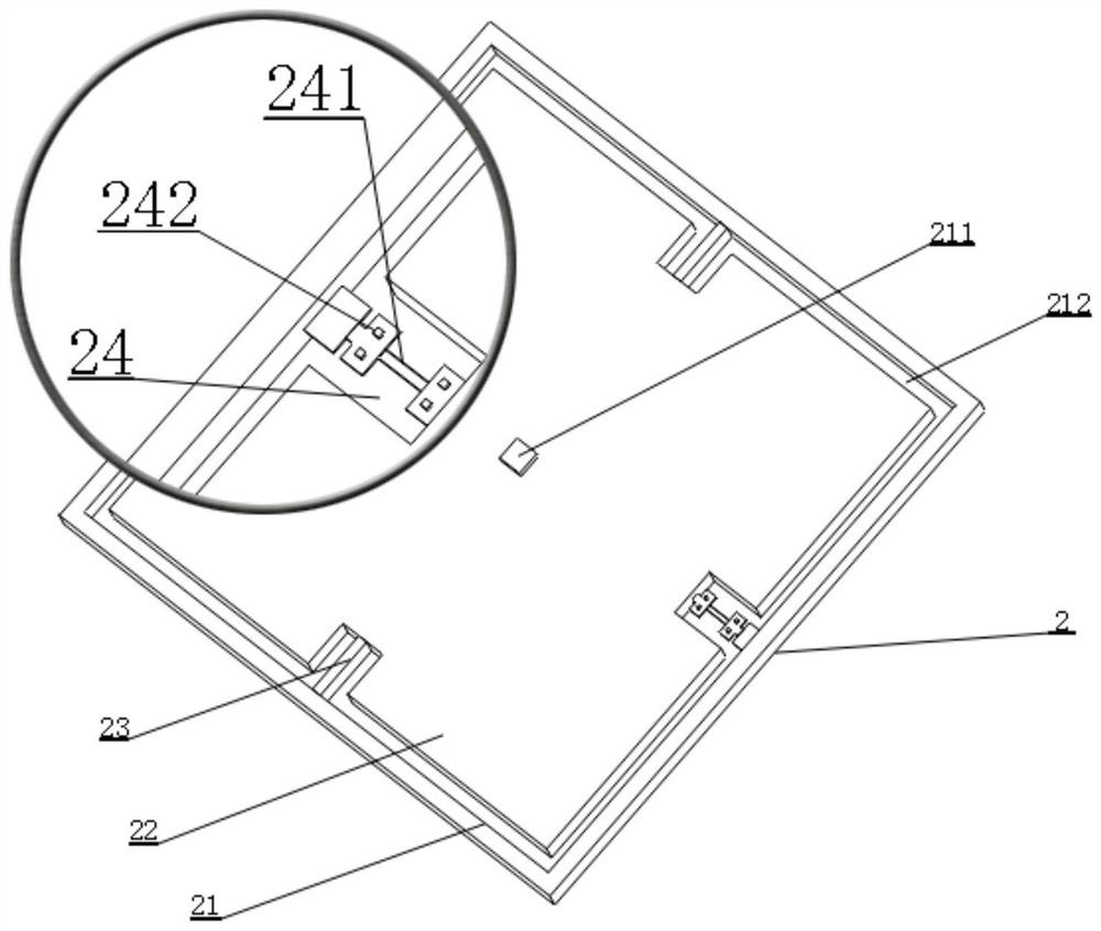
[0056] The detection structure layer 2 is made on the basis of a square double-polished SOI silicon wafer, and includes a square outer frame 21 and a square sensitive mass 22 located in the center of the outer frame 21, and the top surface and the center of the bottom surface of the sensitive mass 22 are respectively provided with Upper limit post 231 and lower limit post 211;
[0057] Taking the center of the sensitive mass 22 as the origin, the two sides of the sensitive mass 22 in the x-axis direction...
Embodiment 2
[0062] The present invention also includes the preparation method of the above-mentioned resonant acceleration sensor based on the nano piezoelectric beam, including the following steps: preparing the chip: taking a double-throwing SOI silicon wafer with a thickness of 100 μm and two crystal orientation N with a thickness of 30 μm Type single throw silicon wafer;
[0063] One-time photolithography: use standard semiconductor cleaning process to clean the double-polished SOI silicon wafer, and spin-coat photoresist on the surface of the double-polished SOI silicon wafer, the photolithography reveals the outer frame 21 and the sensitive mass 22, and the sensitive mass 22 Grooves are respectively photoetched in the middle of each side; as in Figure 5 shown.
[0064] Secondary photolithography: heat the top surface of the double-polished SOI silicon wafer at high temperature to grow a layer of silicon dioxide on the top surface, attach a layer of positive photoresist on the sur...
PUM
| Property | Measurement | Unit |
|---|---|---|
| thickness | aaaaa | aaaaa |
| thickness | aaaaa | aaaaa |
| Resonant frequency | aaaaa | aaaaa |
Abstract
Description
Claims
Application Information


