

Method for enhancing photoetching resolution of dense patterns
A lithography resolution and graphics technology, which is applied in microlithography exposure equipment, photoplate making process of pattern surface, optics, etc., can solve the problems of huge capital cost and uneconomical lithography machine, and achieve the goal of improving resolution Effect
- Summary
- Abstract
- Description
- Claims
- Application Information
AI Technical Summary
Problems solved by technology
Method used
Image

Examples
Embodiment 1
[0034] The method for enhancing the resolution of dense pattern lithography in this embodiment adopts two exposure processes, and the specific process includes:
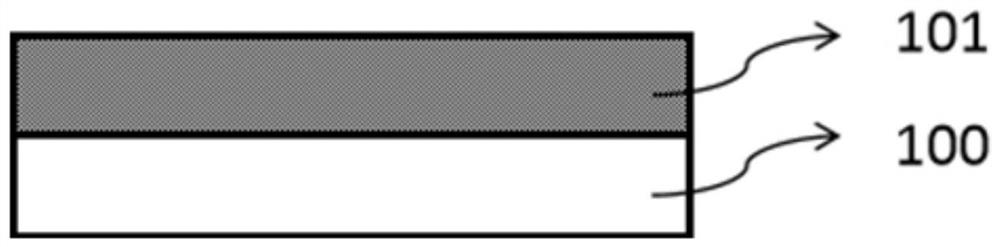
[0035] Uniformly coat a layer of developable glue 101 on the substrate 100 and bake it, such as figure 1 shown.
[0036] The substrate 100 may be monocrystalline silicon, polycrystalline silicon, silicon dioxide, silicon nitride, gallium nitride, gallium arsenide, aluminum oxide, silicon carbide, indium phosphide or other metal or metal alloy substrates.
[0037] Developable rubber 101 is different from photoresist, it has a certain solubility in alkaline developer without exposure, and its dissolution rate can be changed by baking temperature and time. Generally, the dissolution rate in alkaline developer is between 0.1~200nm / s. The developable adhesive 101 is also resistant to dissolution by photoresist solvents. The material of the developable adhesive meeting the above conditions may be a metal lift-off adhes...
Embodiment 2
[0058] The method for enhancing the resolution of dense pattern lithography in this embodiment adopts two exposure processes, and the specific process includes:
[0059] Uniformly coat a layer of developable glue 101 on the substrate 100 and bake it, such as figure 1 shown.
[0060] The substrate 100 may be monocrystalline silicon, polycrystalline silicon, silicon dioxide, silicon nitride, gallium nitride, gallium arsenide, aluminum oxide, silicon carbide, indium phosphide or other metal or metal alloy substrates.
[0061] Developable rubber 101 is different from photoresist, it has a certain solubility in alkaline developer without exposure, and its dissolution rate can be changed by baking temperature and time. Generally, the dissolution rate in alkaline developer is between 0.1~200nm / s. The developable adhesive 101 can also resist dissolution of organic developer and photoresist solvent. The material of the developable adhesive meeting the above conditions may be a meta...
Embodiment 3
[0087] The method for enhancing the resolution of dense pattern lithography in this embodiment adopts two exposure processes, and the specific process includes:
[0088] Uniformly coat a layer of developable glue 101 on the substrate 100 and bake it, such as figure 1 shown.
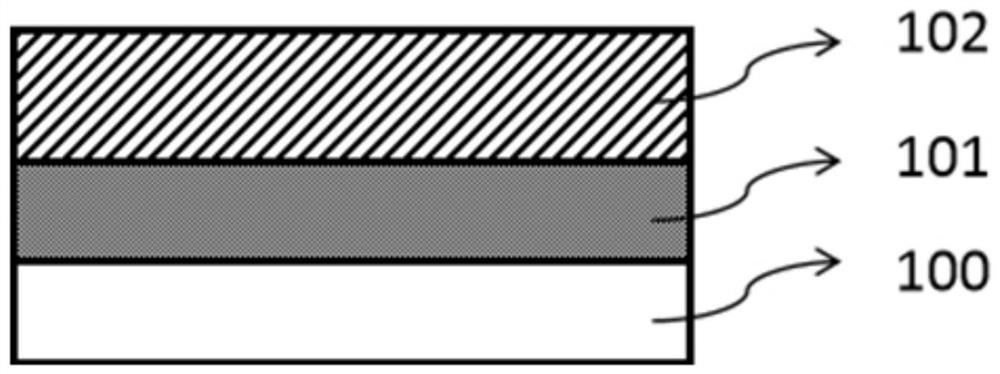
[0089] Uniformly coat a layer of photoresist 102 on the developable glue 101 and bake it, such as figure 2 shown.
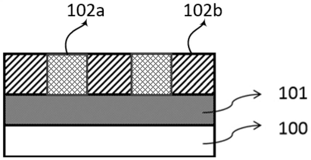
[0090] Through the first photolithography exposure process, based on the mask plate used in this step process, an exposed area 102a and a non-exposed area 102b are formed on the photoresist 102, as image 3 shown.
[0091] Perform post-exposure developing process, use alkaline developing solution to remove the exposed area 102a, meanwhile alkaline developing solution can also dissolve the developable adhesive 101 under the photoresist 102, after a predetermined time, the Figure 4 In the structure shown, the exposed area 102a of the photoresist 102 is dissolved and removed by the alkal...
PUM
 Abstract
Description
Claims
Application Information