
Method for rapidly preparing colloidal photonic crystal array chip by utilizing laser direct writing

A colloidal photonic crystal and chip technology, which is used in crystal growth, optomechanical equipment, microlithography exposure equipment, etc., to achieve the effect of wide application range, simple operation, and avoidance of operating procedures

Inactive Publication Date: 2020-11-13
DALIAN UNIV OF TECH
View PDF5 Cites 1 Cited by
  • Summary
  • Abstract
  • Description
  • Claims
  • Application Information

AI Technical Summary

Problems solved by technology

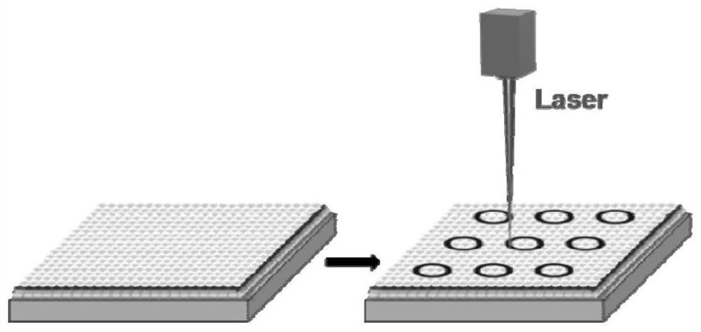
[0004] In order to solve the problems existing in the existing preparation methods, the object of the present invention is to provide a method for rapidly preparing colloidal photonic crystal array chips by using laser direct writing

Method used


Image

  • Method for rapidly preparing colloidal photonic crystal array chip by utilizing laser direct writing
  • Method for rapidly preparing colloidal photonic crystal array chip by utilizing laser direct writing
  • Method for rapidly preparing colloidal photonic crystal array chip by utilizing laser direct writing

Examples


Embodiment 1

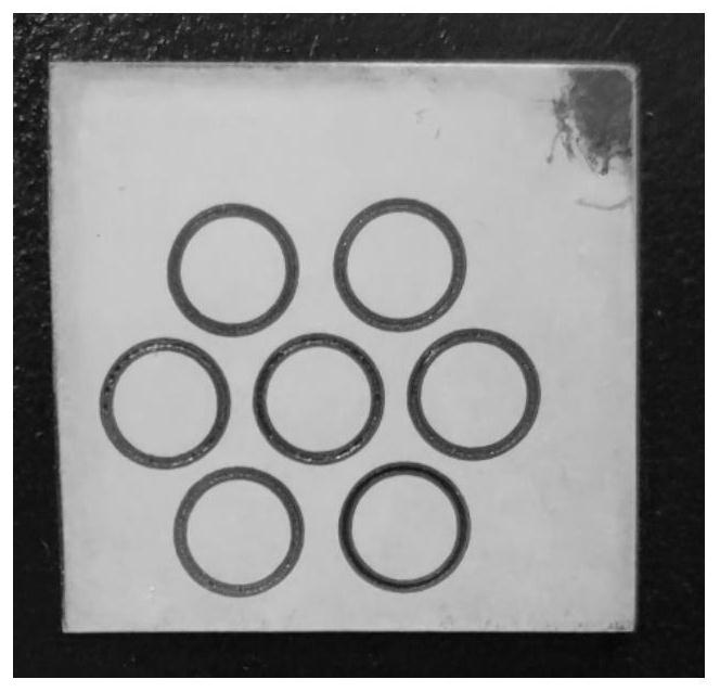
[0025] A method for rapidly preparing a colloidal photonic crystal array chip by using laser direct writing on the surface of a glass substrate, the specific steps are as follows:

[0026] (1) Prepare a square glass sheet with a side length of 2.5 cm as the base material;

[0027] (2) Hydrophilic treatment of the substrate, followed by N 2 blow dry;

[0028] (3) Prepare a polystyrene photonic crystal layer on the substrate;

[0029] (4) Use the software to design the circular array pattern to be etched, and import the file into the carbon dioxide laser device.

[0030] (5) Place the substrate with the photonic crystal layer on the operating table, set the direct writing speed of the carbon dioxide laser to 600mm / s, and the laser power to 12W.

[0031] (6) Start the laser device.

[0032] (7) After the etching is finished, turn off the laser. The colloidal photonic crystal chip ( figure 2 ).

[0033] The method of the invention is easy to prepare, does not need complex ...

Embodiment 2

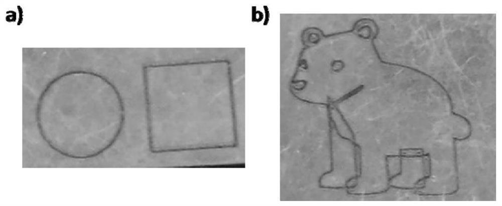
[0035] A method for rapidly preparing a colloidal photonic crystal array chip on the surface of a PMMA substrate using laser direct writing, the specific steps are as follows:

[0036] (1) Prepare a square PMMA sheet with a side length of 2.5 cm as the base material;

[0037] (2) The surface of the substrate is treated with hydrophilicity, and then N 2 blow dry;

[0038] (3) Prepare a polystyrene photonic crystal layer on the substrate;

[0039] (4) Use the software to design the square array pattern to be etched, and import the file into the carbon dioxide laser equipment.

[0040] (5) Place the substrate with the photonic crystal layer on the operating table, set the direct writing speed of the carbon dioxide laser to 600mm / s, and the laser power to 12W.

[0041] (6) Start the laser device.

[0042] (7) After the etching is finished, turn off the laser. Colloidal photonic crystal chips ( image 3 ).


PUM


Abstract

The invention belongs to the technical field of preparation and application of patterned colloidal photonic crystals, and particularly relates to a method for rapidly preparing a colloidal photonic crystal array by utilizing laser direct writing. The method comprises the steps of carrying out modification treatment on the surface of a substrate material so as to enable the surface of the substrateto have super-hydrophilicity or super-hydrophobicity; preparing a colloidal photonic crystal film on the substrate; and placing the substrate with the colloidal photonic crystal film deposited on thesurface under a laser, etching a pre-designed pattern, and cooling at the room temperature. According to the invention, the laser direct writing method is used for preparing the colloidal photonic crystal array chip for the first time, and the preparation method is easy to operate, extremely short in consumed time and wide in application range. The invention provides a feasible new method for rapid and accurate patterned surface preparation in the field of material science by combining the advantages of a rapid and efficient laser direct writing technology and the characteristic that the physical and chemical properties of a polymer photonic crystal material are changed when the polymer photonic crystal material is heated.

Description

technical field [0001] The invention belongs to the technical field of preparation and application of patterned colloidal photonic crystals, and in particular relates to a method for rapidly preparing a colloidal photonic crystal array by using laser direct writing. Background technique [0002] Photonic crystal materials have become commonly used structural color visible light modulation materials and fluorescence enhancement substrate materials in the field of scientific research. Patterned photonic crystals have very important application prospects in the fields of high-sensitivity and high-throughput detection, high-efficiency anti-counterfeiting, and high-performance display devices. [0003] There are currently three main methods for patterning photonic crystals: one is to use patterned substrates for induced assembly. The technologies involved include masking, photolithography, etc. The procedures are cumbersome and complicated, and the operation accuracy is relative...

Claims


Application Information

Patent Timeline
Patent Type & Authority Applications(China)
IPC IPC(8): G03F7/20C30B33/02C30B29/58C30B29/64
CPCC30B29/58C30B29/64C30B33/02G03F7/70383
Inventor 张利静刘博帆杨文博杨琳陶胜洋
Owner DALIAN UNIV OF TECH
Learn More