
A preparation method and application of thin film transistor fine mask

A technology of thin film transistors and mask plates, which is applied in the field of preparation of fine mask plates for thin film transistors, can solve the problems of high manufacturing process costs, and achieve the effects of less process flow, low cost, and high integration

Active Publication Date: 2019-01-15
武汉国创科光电装备有限公司
View PDF4 Cites 0 Cited by
  • Summary
  • Abstract
  • Description
  • Claims
  • Application Information

AI Technical Summary

Problems solved by technology

[0006] Due to the above-mentioned defects and deficiencies, further improvement and improvement are urgently needed in this field, and a method for preparing a fine mask and then a thin film transistor is designed, so that it can overcome the high cost of the traditional small channel preparation process of thin film transistors and the technical difficulties. Complexity, harsh environmental requirements and other shortcomings, can simultaneously prepare the source, drain and channel that meet the precision requirements, simplify the process of preparing a fine mask, and obtain a highly integrated, high-performance thin film transistor device

Method used


Image

  • A preparation method and application of thin film transistor fine mask
  • A preparation method and application of thin film transistor fine mask
  • A preparation method and application of thin film transistor fine mask

Examples


preparation example Construction

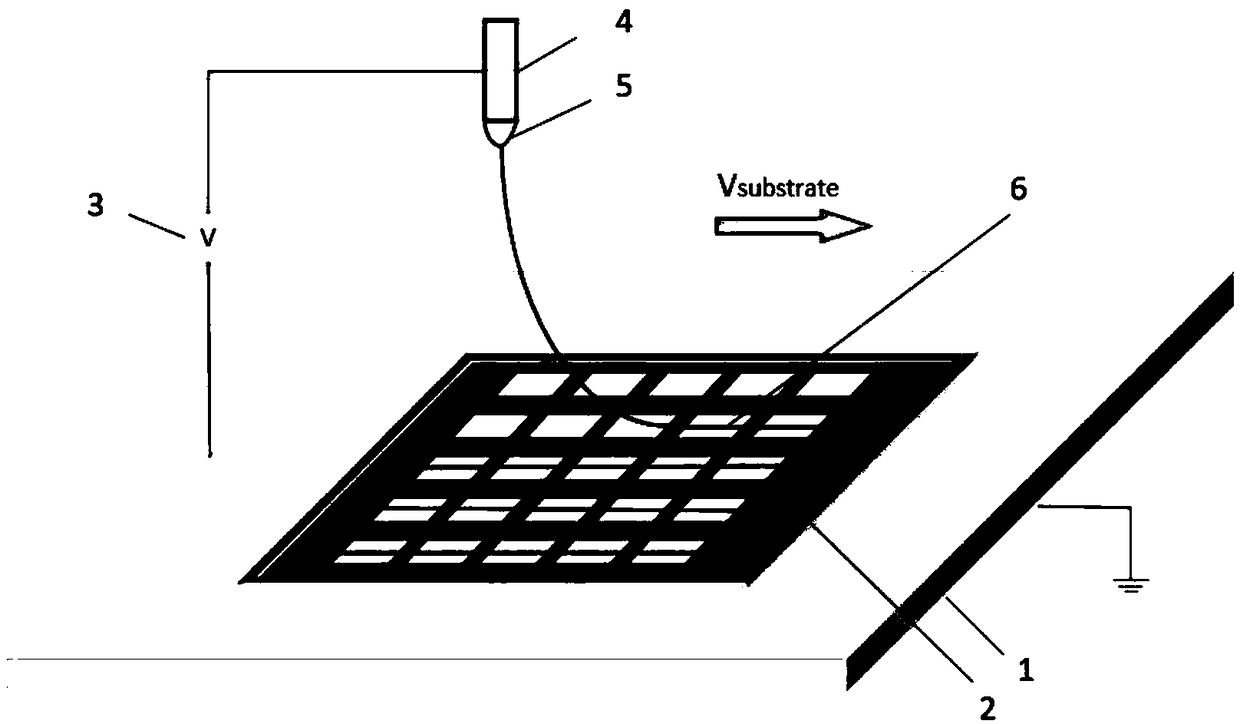
[0036] figure 1Schematic diagram for the preparation of mask plates by electrospinning method. A method for preparing a thin film transistor fine mask according to the present invention specifically comprises the following steps:

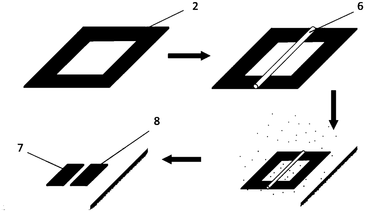
[0037] S1. Prepare a thin metal plate, and etch a plurality of hollow patterns on the thin metal plate, and the hollow patterns are distributed in an array, thereby preparing a hollow metal thin plate;

[0038] S2. Prepare an electrospinning solution for spinning submicron fibers;

[0039] S3. Use the electrospinning solution prepared in step S2 to spin submicron fibers on the thin metal plate prepared in step S1. The single fiber spun spans the hollow part of the thin metal plate, and the hollow part of the thin metal plate is spun. Evenly divided into two adjacent areas;

[0040] S4. After the fibers are solidified, a tube fine mask for preparing thin film crystals composed of metal sheets and fibers is obtained.

[0041] In a preferred embodi...

Embodiment 1

[0056] Utilize process method described in the present invention to manufacture thin film transistor process on silicon substrate as follows:

[0057] (1) Preparation of a semiconductor layer. Add 10mg of P3HT powder to 990mg of chlorobenzene, heat at 70°C, and dissolve with 100W ultrasonic for 1-2h. After the solution has no obvious particles, heat at 60-70°C and magnetically stir for 2-3h to form a uniform semiconductor solution. After standing for 30 minutes, filter with a 0.02um sieve to obtain the prepared organic semiconductor solution. Outsourced silicon oxide wafer, in which N++Si is the gate, with a thickness of about 200 μm, such as image 3 As shown in middle 9, SiO2 is an insulating layer with a thickness of about 100nm, such as image 3 Shown in 10. The semiconductor solution is spin-coated on the surface of the SiO2 insulating layer, the rotation speed is 1500r / min, and the time is 75s. The thickness of the obtained P3HT film is generally controlled between 50...

Embodiment 2

[0061] The process of manufacturing a flexible thin film transistor using the process method described in the present invention is as follows:

[0062] (1) Prepare the metal grid. Cut the PI film with a thickness of 30-50 μm into a square of 10 cm × 10 cm, ultrasonically clean it with acetone, absolute ethanol, and deionized water for 10 min, and finally dry it with nitrogen. Use the method of thermal evaporation coating to plate gold on the cleaned PI film with a thickness of 100-300nm, such as Figure 4 Shown in 13.

[0063] (2) Prepare an insulating layer. Dissolve an appropriate amount of polymethyl methacrylate (PMMA) in a chlorobenzene solution to form a solution of 5-10 mg / ml, and spin-coat it on the surface of the gate at a speed of 1000 r / min for 60 seconds, and control the thickness at 100~ 300nm, dry the film at 100°C-150°C after spin coating, such as Figure 4 Shown in 14.

[0064] (3) Preparation of an organic semiconductor layer. Add 10mg of P3HT powder to ...


PUM

PropertyMeasurementUnit
diameteraaaaaaaaaa
diameteraaaaaaaaaa
thicknessaaaaaaaaaa

Abstract

The invention belongs to the technical field of semiconductor and electrospray printing, and specifically relates to a preparation method of a thin film transistor fine mask and a method for preparing a thin film transistor using the mask. Spinning technology prepares fibers across the hollow part on the metal sheet, so that the hollow part is divided into two regions with a pitch of submicron or even nanometer. Using the thin metal plate printed with fibers as a mask, the source and drain are simultaneously constructed on the semiconductor layer by evaporation or sputtering. The channel length between the source and drain is slightly smaller than the fiber diameter, and the fiber diameter width can be realized The range is 50nm-30μm, so that a TFT device with excellent performance can be obtained. The method for preparing a fine mask plate proposed by the present invention and the method for preparing a thin film transistor using the fine mask plate have less process flow and low cost, and can realize large-area and array-based preparation, which is conducive to obtaining highly integrated and high-performance thin film transistor devices .

Description

technical field [0001] The invention belongs to the technical field of semiconductor and electrospray printing, and in particular relates to a method for preparing a thin film transistor fine mask and its application, which can simultaneously prepare the source and the drain, and prepare a nanoscale The channel satisfies the precision requirements for the fabrication of thin film transistors. Background technique [0002] Thin Film Transistor (TFT), as a basic component of microelectronics, has broad application prospects in flexible display, wearable electronics, microsensors and other fields. With the development of microelectronics technology, the performance and integration of TFT are getting higher and higher, and the feature size is shrinking, which poses many challenges to its design and manufacture. [0003] The preparation method of the source and drain of the transistor is mainly radio frequency sputtering or thermal evaporation. The channel length between the sou...

Claims


Application Information

Patent Timeline
Patent Type & Authority Patents(China)
IPC IPC(8): H01L51/05H01L51/40C23C14/04
CPCC23C14/042H10K71/166H10K10/466
Inventor 黄永安段永青邵志龙丁亚江尹周平徐洲龙
Owner 武汉国创科光电装备有限公司
Learn More