Method for preparing two-dimensional transverse heterojunction on transition metal chalcogenide matrix based on selective reaction
A technology of chalcogen compounds and transition metals, applied in metal material coating technology, semiconductor/solid-state device manufacturing, semiconductor devices, etc., can solve problems such as not suitable for large-scale growth and low efficiency
- Summary
- Abstract
- Description
- Claims
- Application Information
AI Technical Summary
Problems solved by technology
Method used
Image
Examples
Embodiment 1
[0057] Fabrication of transition metal chalcogenide thin films on substrates:
[0058] a1) SiO 2 -Si substrate is used as the substrate, and the thickness of silicon oxide is 300nm. The substrate is placed in deionized water, acetone and isopropanol for ultrasonic cleaning, and then dried with nitrogen; 3 In a double-ended open quartz boat, placed in the tube furnace reaction chamber;
[0059] b1) placing a quartz boat equipped with sulfur powder in the heating zone upstream of the air flow at the base;
[0060] c1) After scrubbing with argon gas in the tube furnace, feed 5 sccm of argon gas, and after the gas flow is stable, the sulfur powder and MoO 3 Heating to temperatures of 130-140°C and 645-655°C respectively, and keeping the temperature constant for 5-10 minutes, to obtain a single layer of MoS grown on the substrate 2 Thin film, the film thickness is 0.7nm.
Embodiment 2
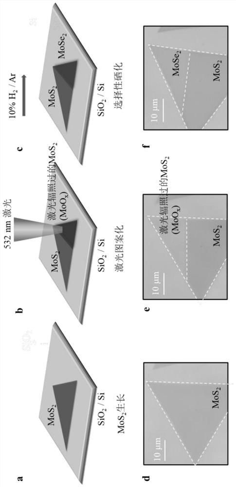
[0062] attached figure 1 a-1c shows a schematic diagram of the preparation process of the heterojunction, which is synthesized and prepared according to the process shown in the figure.
[0063] Preparation of MoS 2 -MoSe 2 The specific steps of heterojunction are as follows:
[0064] 1) Laser direct writing process:
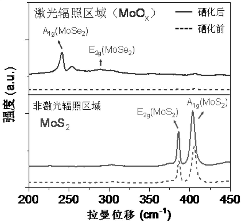
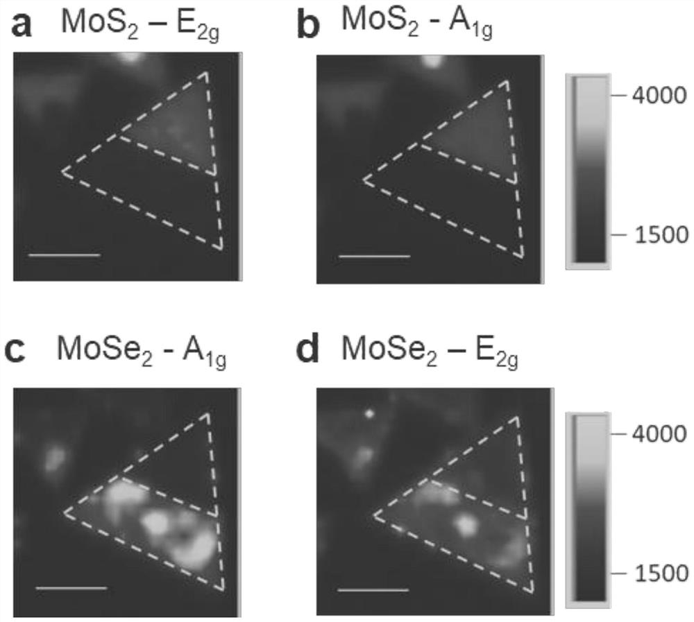
[0065] Use the required graphics with the software for laser direct writing equipment, use the TANGO translation stage and control software, and use the single-layer MoS grown on the substrate of Example 1 2 The thin film is placed at the starting point of the scanned image, and a laser with a wavelength of 532nm is used to follow the specified path of the required pattern at a rate of 20.4kW / mm 2 power and rate of 10 μm / s in monolayer MoS 2 The surface of the film is irradiated and scanned, and ultra-thin, highly reactive, and patterned MoO is obtained after scanning x Oxidized regions, oxidized regions (TMO) and non-oxidized regions (TMD) together form M...
Embodiment 3
[0075] Unlike ordinary CVD growth methods, which can only grow on the active sites on the edge or face, since the growth precursor here is the TMO region that has been laser patterned, this region is only atomically thick and because it is rich in Due to the high reactivity due to defects, the reduction reaction can occur at a growth temperature that is about 50-200 ° C lower than that of conventional methods. At this time, the TMD region (non-oxidation region) can remain intact because it does not reach the reaction temperature of the conventional synthesis method using powder oxide as a precursor. Therefore, this reaction process is highly selective, and the reaction only occurs in the TMO region.
[0076] The invention overcomes the complex graphics and graphics with radians that cannot be realized by the traditional CVD growth method, Figure 7 , Figure 8 , Figure 9 and Figure 10 Heterojunction materials with different patterns prepared by this method are shown, inc...
PUM
| Property | Measurement | Unit |
|---|---|---|
| thickness | aaaaa | aaaaa |
| thickness | aaaaa | aaaaa |
| thickness | aaaaa | aaaaa |
Abstract
Description
Claims
Application Information


