Top-emitting OLED device with cathode single-sided grating and preparation method thereof

A top emission and grating technology, applied in the field of top emission OLED devices and their preparation, can solve the problems of preparing gratings and the like, and achieve the effects of less process, low cost, and improved luminous efficiency

Active Publication Date: 2019-01-01
武汉国创科光电装备有限公司
View PDF2 Cites 4 Cited by
  • Summary
  • Abstract
  • Description
  • Claims
  • Application Information

AI Technical Summary

Problems solved by technology

Using electrofluid jet printing technology to fabricate nano-gratings on the surface of OLED cathodes will not damage the prepared functional structure, which is a good solution to the problem that it is difficult to directly fabricate gratings on the surface of OLED cathodes with existing micro-nano processing technology

Method used


Image

  • Top-emitting OLED device with cathode single-sided grating and preparation method thereof
  • Top-emitting OLED device with cathode single-sided grating and preparation method thereof
  • Top-emitting OLED device with cathode single-sided grating and preparation method thereof

Examples


Embodiment 1

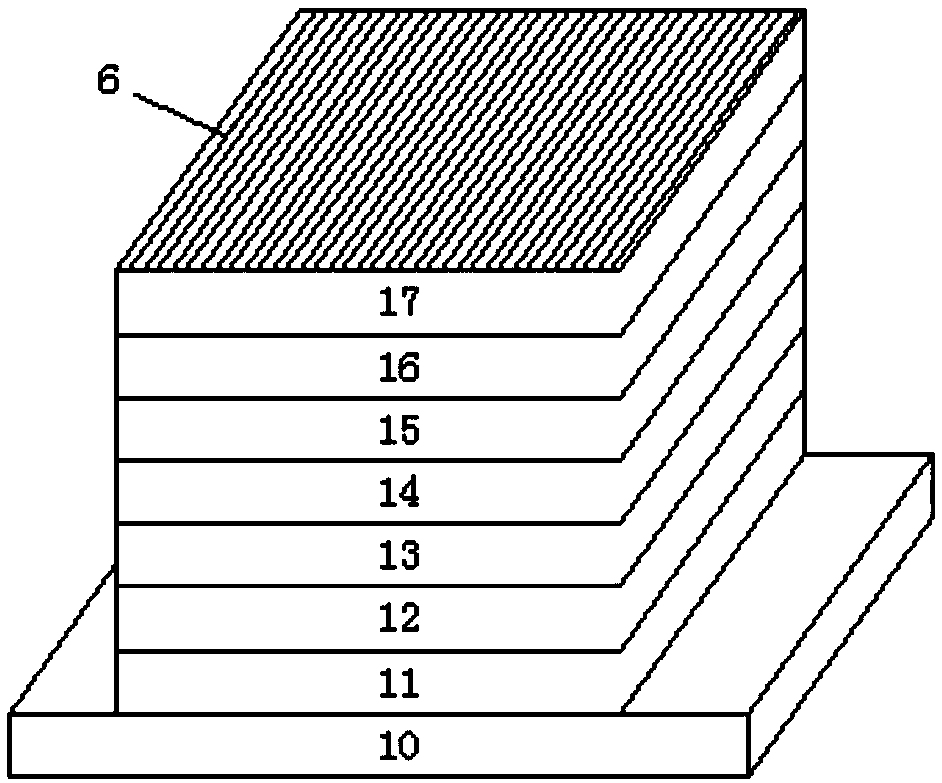
[0035] 1) Prepare the substrate 10, which is an ITO-coated glass substrate. Sonicate with acetone, absolute ethanol, and deionized water for 10 minutes, then blow dry with nitrogen, and finally heat in a vacuum oven at 80° C. for 30 minutes.

[0036] 2) Preparation of a top-emitting OLED device 2 suitable for monochromatic green light. The existing commonly used green OLED structure is adopted. in 3×10 -4 100nm Al is vapor-deposited under Pa pressure environment to form metal anode 11, and then successively vapor-deposits 10nm molybdenum trioxide (MoO 3) as hole injection layer 12, 52 nm of N,N'-diphenyl-N,N'-(1-naphthyl)-1,1'-biphenyl-4,4'-diamine (NPB) as Hole transport layer 13, 20nm 8-hydroxyquinoline aluminum (Alq 3 ) as the OLED light-emitting layer 14 suitable for green light, 15nm phenanthroline (BPhen) doped with lithium (Li) (BPhen: Li) as the electron injection layer 16 to reduce the electron injection barrier and improve conductivity. 10nm of BPhen is used as t...

Embodiment 2

[0041] 1) Prepare the substrate 10, which is an ITO glass substrate. Sonicate with acetone, absolute ethanol, and deionized water for 20 minutes respectively, then blow dry with nitrogen, and finally heat in a vacuum oven at 90° C. for 20 minutes.

[0042] 2) Preparation of a top-emitting OLED device 2 suitable for white light. The existing common white light OLED structure is adopted. at 3×10 - 4 The metal anode 11 is formed by evaporating 100nm Al under Pa pressure environment, and then depositing a hole injection layer 12 with a thickness of 5nm in sequence. Triphenylamine) is formed, 40nm thick hole transport layer 13, hole transport layer 13 adopts TAPC (two-[4-(N,N-xylyl-amino)-phenyl] cyclohexane) to form, redeposition OLED light-emitting layer 14, OLED light-emitting layer 14 includes a 19nm-thick blue light unit and a 1nm-thick yellow light unit, which can emit white light. Pyridyl)phenyl-(2-carboxypyridyl)iridium(III)) is doped with host material mCP(N,N′-dicarba...

Embodiment 3

[0047] 1) Prepare the substrate 10, the substrate 10 is an ITO glass substrate, ultrasonically use acetone, absolute ethanol, and deionized water for 30 minutes, then blow dry with nitrogen, and finally heat in a vacuum oven at 100°C for 10 minutes .

[0048] 2) Preparation of a top-emitting OLED device 2 suitable for white light. The existing common white light OLED structure is adopted. at 3×10 - 4 The metal anode 11 is formed by evaporating 100nm Al under Pa pressure environment, and then depositing a hole injection layer 12 with a thickness of 5nm in sequence. Triphenylamine) is formed, 40nm thick hole transport layer 13, hole transport layer 13 adopts TAPC (two-[4-(N,N-xylyl-amino)-phenyl] cyclohexane) to form, redeposition OLED light-emitting layer 14, OLED light-emitting layer 14 includes a 19nm-thick blue light unit and a 1nm-thick yellow light unit, which can emit white light. Pyridyl)phenyl-(2-carboxypyridyl)iridium(III)) is doped with host material mCP(N,N′-dic...


PUM

PropertyMeasurementUnit
diameteraaaaaaaaaa
diameteraaaaaaaaaa
diameteraaaaaaaaaa

Abstract

The invention belongs to the field of organic light-emitting diodes, and discloses a preparation method of a top-emitting OLED device with a cathode single-sided grating. The preparation method comprises the following steps: 1) cleaning a substrate and heating the substrate in a vacuum oven; 2) depositing a metal anode on the upper surface of the substrate, then depositing an organic composite layer on the upper surface of the metal anode, and then depositing a metal cathode on the organic composite layer; 3) printing a grating on the upper surface of the prepared metal cathode by using an electrofluid spray printing solution; and 4) enclosing the organic composite layer with epoxy resin, and bonding a glass cover plate with the substrate by using the epoxy resin, thus completing packaging. The top-emitting OLED device with a cathode single-sided grating and the preparation method thereof maintain the excellent electrical conductivity and microcavity effect of a planar device, stimulates the surface plasmon coupling to emit light, so as to greatly improve the light emitting efficiency. The preparation method of the grating can be applied to large-area and array preparation, and isbeneficial to industrial production.

Description

technical field [0001] The invention belongs to the field of organic light-emitting diodes, and more specifically relates to a top-emitting OLED device and a preparation method thereof. Background technique [0002] Organic light-emitting diodes (OLEDs) have the advantages of fast response speed, low driving voltage, solid-state active light emission, wide viewing angle, bendable / foldable, etc., and have great application prospects and market value in the fields of solid-state lighting and flat panel display. OLED technology has made great breakthroughs in recent years, but luminous efficiency has always been the main factor limiting its development, how to improve the light extraction efficiency of OLED devices is very important. [0003] The total reflection caused by the waveguide mode and the loss of surface plasmons are the main factors affecting the light extraction efficiency of OLED devices, resulting in the external quantum efficiency of OLED devices usually only re...

Claims


Application Information

Patent Timeline
Patent Type & Authority Applications(China)
IPC IPC(8): H01L51/52H01L51/50H01L51/56
CPCH10K50/00H10K50/85H10K71/00H10K2102/3026
Inventor 段永青尹周平李禾耕李华阳
Owner 武汉国创科光电装备有限公司
Why Eureka
Try Eureka