Multi-layer phase change film based on alternate stacking of germanium antimony telluride and IV group telluride and application thereof
A germanium antimony telluride and telluride technology, applied in the field of multilayer phase-change thin films, can solve the problems that hinder the application of general-purpose memory and brain-like computing chips, reduce the stability and accuracy of devices, and stabilize service, so as to increase the production cost and the difficulty of preparation, improving stability and accuracy, and ensuring the effect of reliability
- Summary
- Abstract
- Description
- Claims
- Application Information
AI Technical Summary
Problems solved by technology
Method used
Image

Examples
preparation example Construction
[0033] The phase change film can be prepared by sputtering, evaporation, chemical vapor deposition, plasma enhanced chemical vapor deposition, low pressure chemical vapor deposition, metal compound vapor deposition, molecular beam epitaxy, atomic vapor deposition and atomic Any of the layer deposition methods.
[0034] The phase change thin film can realize phase change through electrical pulse or optical pulse, and can be applied in the field of phase change memory and brain-inspired computing chip.
Embodiment 1
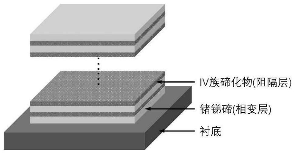
[0037] A based on GeSbTe and TiTe 2 Alternately stacked phase-change films, the films comprising:
[0038] GeSbTe material as phase change layer and TiTe as barrier layer 2Alternate stacking of materials, including 2 layers of GeSbTe film and 1 layer of TiTe 2 film;
[0039] The thickness of each layer of GeSbTe film is about 2nm, each layer of TiTe 2 The thickness of the film is about 1nm, and the overall thickness of the film is about 5nm;
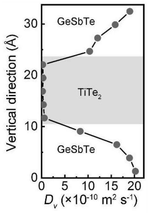
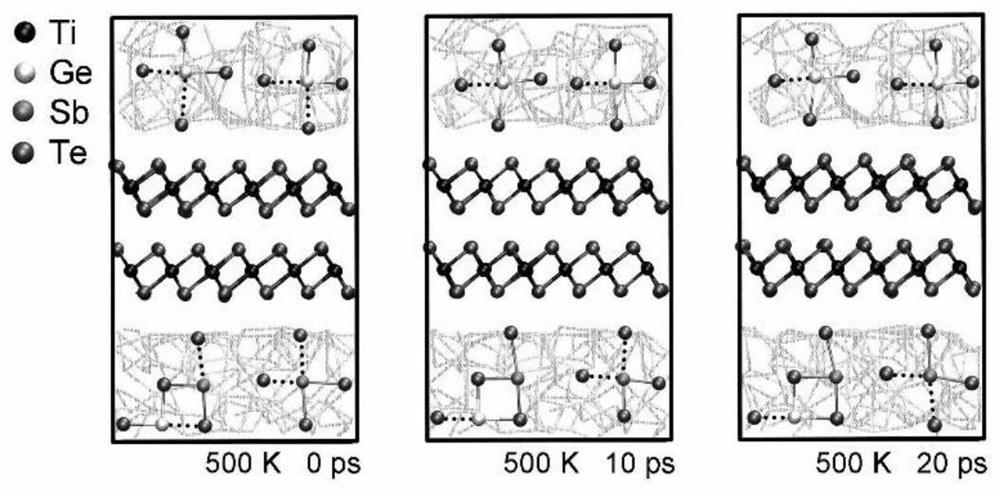
[0040] Among them GeSbTe and TiTe 2 Both have an octahedral structure, and the van der Waals force is formed between adjacent layers to form a van der Waals layer. When GeSbTe is crystallized, TiTe 2 It can be used as a template to speed up the crystallization process of GeSbTe and increase its phase transition rate;
[0041] Under the action of electrical or optical pulses, the GeSbTe layer undergoes phase transition, and there are at least three stable signal resistance states, including amorphous state, metastable state (cubic p...
Embodiment 2
[0047] A based on GeSbTe and ZrTe 2 Alternately stacked phase-change films, the films comprising:
[0048] GeSbTe material as phase change layer and ZrTe as barrier layer 2 Alternate stacking of materials, including 5 layers of GeSbTe film and 4 layers of ZrTe 2 film;
[0049] The thickness of each layer of GeSbTe film is 7nm, each layer of TiTe 2 The thickness of the film is 2nm, and the overall thickness of the film is about 43nm;
[0050] Among them GeSbTe and ZrTe 2 Both are octahedral structures, and van der Waals forces form van der Waals layers between adjacent layers. When GeSbTe is crystallized, ZrTe 2 It can be used as a template to speed up the crystallization process of GeSbTe and increase its phase transition rate;
[0051] Under the action of electrical or optical pulses, the GeSbTe layer undergoes phase transition, and there are at least three stable signal resistance states, including amorphous state, metastable state (cubic phase) and stable state (hexag...
PUM
| Property | Measurement | Unit |
|---|---|---|
| Thickness | aaaaa | aaaaa |
Abstract
Description
Claims
Application Information