
Preparation method of electro-optical crystal film, electro-optical crystal film and electro-optical modulator

An electro-optical crystal and thin-film technology, applied in light guide, optics, instruments, etc., can solve problems such as affecting the performance of electro-optical modulators, affecting the propagation of optical signals, and the inability of silicon materials and lithium niobate crystals to be fully bonded.

Pending Publication Date: 2020-11-20
JINAN JINGZHENG ELECTRONICS
View PDF8 Cites 7 Cited by
  • Summary
  • Abstract
  • Description
  • Claims
  • Application Information

AI Technical Summary

Problems solved by technology

[0005] This application provides a method for preparing electro-optic crystal thin films, electro-optic crystal thin films and electro-optic modulators to solve the problem of using benzocyclobutene resin as an adhesive to combine silicon materials with lithium niobate crystals in the prior art. Silicon materials and lithium niobate crystals cannot be completely bonded, which affects the propagation of optical signals, which in turn affects the performance of electro-optic modulators

Method used


Image

  • Preparation method of electro-optical crystal film, electro-optical crystal film and electro-optical modulator
  • Preparation method of electro-optical crystal film, electro-optical crystal film and electro-optical modulator
  • Preparation method of electro-optical crystal film, electro-optical crystal film and electro-optical modulator

Examples


preparation example Construction

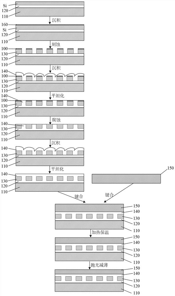
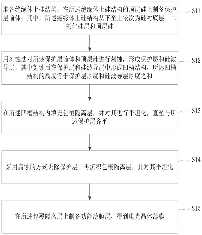
[0032] Specifically, such as figure 2 Shown, described preparation method comprises the following steps:

[0033] S11, preparing the SOI structure, depositing a protective layer precursor 160 on the top silicon layer of the SOI structure; wherein, the SOI structure is sequentially composed of a silicon substrate layer 110, a silicon dioxide layer 120 and a top layer of silicon Si from bottom to top.

[0034] In this step, the silicon-on-insulator structure is also called SOI wafer, and the SOI wafer structure from top to bottom is: 50nm-50μm Si / , 50nm-5μm SiO 2 / Si, use LPCVD to deposit a protective layer precursor 160 on the top layer of silicon Si, the thickness of which can be 20nm-2000nm. Of course, PECVD or thermal oxidation method can also be used for depositing the protective layer precursor 160, which is not specifically limited in this step.

[0035]S12, using an etching method to etch the protective layer precursor 160 and the top layer of silicon Si to form the pr...

Embodiment 1

[0076] Embodiment 1 (ion implantation+bonding separation method)

[0077] 1) Prepare an SOI wafer with a size of 4 inches, a thickness of 0.5mm and a smooth surface. The structure of the SOI wafer is 220nm Si / 2μm SiO from top to bottom 2 / Si, cleaning the top layer silicon (Si) of the SOI wafer, and then using LPCVD to deposit a layer of silicon nitride (SiNx) as a protective layer precursor, wherein the thickness of SiNx is 50nm.

[0078] 2) Etching the protective layer precursor and the top layer of silicon on the side of the wafer containing the protective layer precursor described in step 1) using a dry etching method to form a protective layer and a silicon waveguide layer. The silicon on the top layer is completely etched through and etched into a ridge-shaped silicon waveguide. Finally, a groove structure is formed in the protection layer and the silicon waveguide layer, and the height of the groove structure is equal to the sum of the thickness of the protection layer...

Embodiment 2

[0087] Embodiment 2 (method of direct bonding+grinding and polishing)

[0088] 1) Prepare an SOI wafer with a size of 4 inches, a thickness of 0.5mm and a smooth surface. The structure of the SOI wafer is 220nm Si / 2μm SiO from top to bottom 2 / Si, cleaning the top Si layer of the SOI wafer, and then using LPCVD to deposit a layer of silicon carbide as a protective layer precursor, wherein the thickness of silicon carbide is 50nm.

[0089] 2) Etching the protective layer precursor and the top layer of silicon on the side of the wafer containing the protective layer precursor described in step 1) using a dry etching method to form a protective layer and a silicon waveguide layer. The top layer of silicon is not completely etched through, and etched into a ridge-shaped silicon waveguide. Finally, a groove structure is formed in the protection layer and the silicon waveguide layer, and the height of the groove structure is equal to the sum of the thickness of the protection layer...


PUM

PropertyMeasurementUnit
surface roughnessaaaaaaaaaa
surface smoothnessaaaaaaaaaa
thicknessaaaaaaaaaa

Abstract

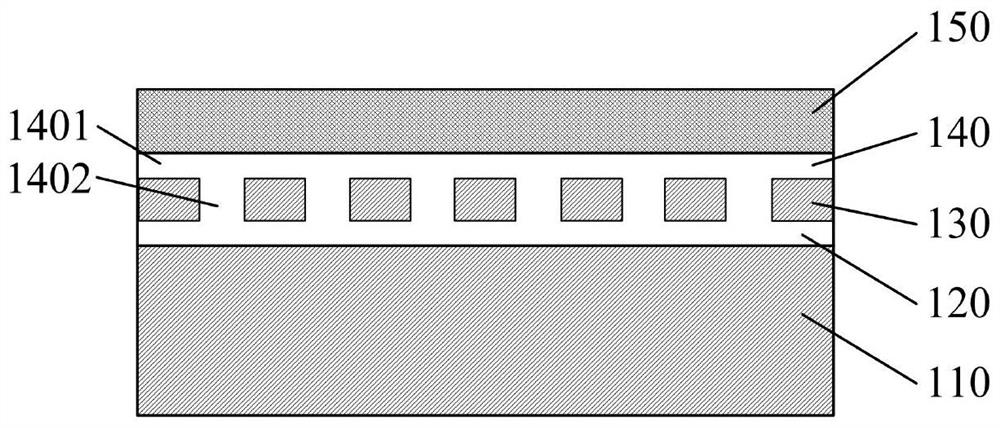
The invention provides a preparation method of an electro-optical crystal thin film, the electro-optical crystal thin film and an electro-optical modulator, and the preparation method of the electro-optical crystal thin film comprises the following steps: preparing a silicon-on-insulator structure, and preparing a protective layer precursor on top silicon of the silicon-on-insulator structure; etching the protective layer precursor and the top silicon layer by using an etching method to form a protective layer and a silicon waveguide layer, forming a groove structure in the protective layer and the silicon waveguide layer after etching, and enabling the height of the groove structure to be equal to the sum of the thickness of the protective layer and the thickness of the silicon waveguidelayer; filling and coating an isolation layer in the groove structure, and flattening the isolation layer until the isolation layer is flush with the protection layer; removing the protective layer ina corrosion manner, depositing and coating the isolation layer, and flattening the isolation layer; and finally, preparing a functional film layer on the coating isolation layer to obtain the electro-optic crystal film. By adopting the scheme, the silicon waveguide layer is protected by the protective layer, the thickness of the coated isolation layer is controllable, the surface is smooth, the coated isolation layer is bonded with the functional film layer, and the propagation of optical signals is not influenced.

Description

technical field [0001] The present application relates to the field of semiconductor technology, in particular to a method for preparing an electro-optic crystal thin film, an electro-optic crystal thin film and an electro-optic modulator. Background technique [0002] At present, the processing technology of silicon materials is very mature, and it is also a semiconductor material with more industrial applications. Therefore, silicon materials have been widely used in electronic components. Since the silicon material itself has a centrosymmetric crystal structure, there is no linear electro-optic effect in silicon, so the silicon material cannot be directly used to prepare high-performance electro-optic modulators. For this reason, traditional silicon-based electro-optic modulators usually need to rely on the plasma dispersion effect to solve the above problems. The specific method is to use ion implantation to form a PN junction, and change the silicon density in the silic...

Claims


Application Information

Patent Timeline
Patent Type & Authority Applications(China)
IPC IPC(8): G02F1/035G02F1/03G02B6/122G02B6/136
CPCG02F1/035G02F1/0311G02B6/122G02B6/136G02B2006/12142
Inventor 张秀全王金翠刘桂银李真宇张涛杨超
Owner JINAN JINGZHENG ELECTRONICS
Learn More