
Two-dimensional tungsten disulfide self-configuration homojunction, preparation method and application thereof

A technology of tungsten disulfide and homojunction, applied in chemical instruments and methods, inorganic chemistry, tungsten compounds, etc., can solve problems such as difficult-to-control material thickness, large surface defects, etc., achieve good crystallization, improve quality, and short growth time Effect

Active Publication Date: 2020-12-15
GUANGDONG UNIV OF TECH
View PDF6 Cites 5 Cited by
  • Summary
  • Abstract
  • Description
  • Claims
  • Application Information

AI Technical Summary

Problems solved by technology

[0004] At present, most researchers use the transfer method or the extension growth method to build the homojunction of tungsten disulfide when studying the homojunction, which will Makes there are larger surface defects between the two layers of material, and it is more difficult to control the thickness of the material
At present, no one at home and abroad has successfully made a self-structural homogeneous structure of two-dimensional tungsten disulfide with good crystallinity.

Method used


Image

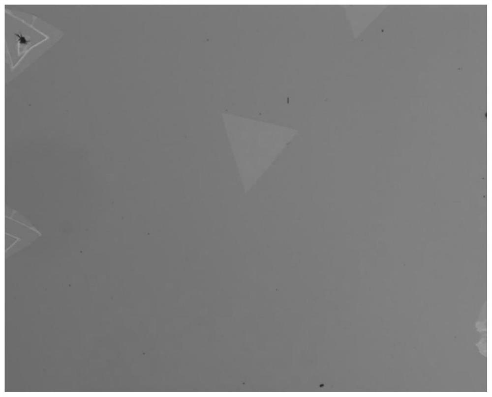
  • Two-dimensional tungsten disulfide self-configuration homojunction, preparation method and application thereof
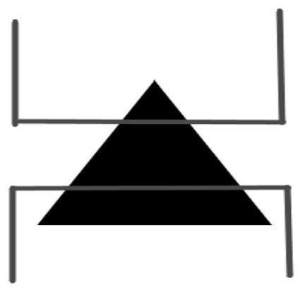
  • Two-dimensional tungsten disulfide self-configuration homojunction, preparation method and application thereof
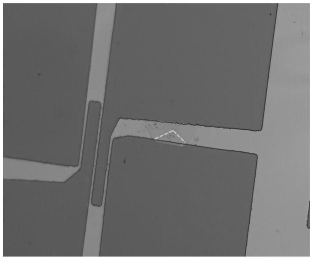
  • Two-dimensional tungsten disulfide self-configuration homojunction, preparation method and application thereof

Examples


Embodiment 1

[0053] (1) Select a size of 1cm 2 For a square silicon dioxide silicon wafer, put it into acetone, absolute ethanol, and deionized water for 5 minutes, then rinse it with deionized water, and quickly dry it with nitrogen; Hydrophilic surface treatment of nitrogen: Put the silicon dioxide silicon wafer into the plasma degumming machine, turn on the pneumatic N with an air pressure of 6bar 2 The valve is filled and then opened with process gas O at 1.5 bar 2Plasma treatment is performed on the valve to obtain pretreated silicon dioxide silicon wafers; 1.5g of tungsten disulfide powder (purity of more than 99.9%) is placed on a clean quartz boat, and the pretreated silicon dioxide silicon wafers are laid flat In another clean quartz boat, place the quartz boat containing tungsten disulfide powder in the middle of the tube furnace, and place the quartz boat loaded with pretreated silica wafers downstream of the tube furnace , the placement position is that the silicon wafer is i...

Embodiment 2

[0062] (1) Select a size of 1cm 2 For a square silicon dioxide silicon wafer, put it into acetone, absolute ethanol, and deionized water for 5 minutes, then rinse it with deionized water, and quickly dry it with nitrogen; Hydrophilic surface treatment of nitrogen: Put the silicon dioxide silicon wafer into the plasma degumming machine, turn on the pneumatic N with an air pressure of 6bar 2 The valve is filled and then opened with process gas O at 1.5 bar 2 The valve is subjected to Plasma treatment to obtain a pretreated silicon dioxide silicon wafer; 1g of tungsten disulfide powder (purity of more than 99.9%) is placed on a clean quartz boat, and the pretreated silicon dioxide silicon wafer is placed flat on the In another clean quartz boat, place the quartz boat containing tungsten disulfide powder in the middle of the tube furnace, and place the quartz boat loaded with the pretreated silicon dioxide wafers downstream of the tube furnace. The placement position is that the...

Embodiment 3

[0070] (1) Select a size of 1cm 2 For a square silicon dioxide silicon wafer, put it into acetone, absolute ethanol, and deionized water for 5 minutes, then rinse it with deionized water, and quickly dry it with nitrogen; Hydrophilic surface treatment of nitrogen: Put the silicon dioxide silicon wafer into the plasma degumming machine, turn on the pneumatic N with an air pressure of 6bar 2 The valve is filled and then opened with process gas O at 1.5 bar 2 The valve is subjected to Plasma treatment to obtain a pretreated silicon dioxide silicon wafer; 2g of tungsten disulfide powder (purity of more than 99.9%) is placed on a clean quartz boat, and the pretreated silicon dioxide silicon wafer is placed flat on the In another clean quartz boat, place the quartz boat containing tungsten disulfide powder in the middle of the tube furnace, and place the quartz boat loaded with the pretreated silicon dioxide wafers downstream of the tube furnace. The placement position is that the...


PUM


Abstract

The invention belongs to the technical field of two-dimensional material heterojunction optical detection, and particularly relates to a two-dimensional tungsten disulfide self-configuration homojunction, a preparation method and application thereof. The preparation method includes: placing tungsten disulfide powder in the middle of a tube furnace through a physical vapor deposition method, and placing a silicon wafer with silicon dioxide on the surface on the downstream of the tube furnace; in a nitrogen atmosphere, raising the temperature to 1100-1150DEG C, carrying out reverse ventilation before the heat preservation temperature is reached to obtain a silicon wafer grown with two-dimensional tungsten disulfide, then performing photoresist spin coating, heating and photoetching on the silicon wafer, controlling the channel width of a photoetching plate to fold two-dimensional tungsten disulfide, then performing development, then building electrodes at two ends of a homojunction successfully, thus obtaining the two-dimensional tungsten disulfide self-configuration homojunction, which has a good optical detection application prospect.

Description

technical field [0001] The invention belongs to the technical field of two-dimensional material heterojunction optical detection, and in particular relates to a two-dimensional tungsten disulfide self-structured homojunction and its preparation method and application. Background technique [0002] Physical Vapor Deposition (Physical Vapor Deposition, PVD) technology refers to the use of physical methods under vacuum conditions to vaporize the material source—solid or liquid surface into gaseous atoms, molecules or parts of ionization into ions, and pass through low-pressure gas (or plasma) ) process, the technology of depositing a thin film with a certain special function on the surface of the substrate. [0003] Two-dimensional tungsten disulfide is a graphite-like layered material with a layer spacing of 0.7nm. WS 2 The single-layer structure metal W atomic layer is sandwiched between the upper and lower layers of S atomic layers. The W atoms and S atoms are bonded by st...

Claims


Application Information

Patent Timeline
Patent Type & Authority Applications(China)
IPC IPC(8): C01G41/00H01L31/032H01L31/103H01L31/18
CPCC01G41/00H01L31/18H01L31/103H01L31/032C01P2004/01C01P2006/40Y02P70/50
Inventor 周瑜琛郑照强
Owner GUANGDONG UNIV OF TECH
Learn More