Functionalized wide-width implanted microelectrode array, manufacturing method and application thereof

A micro-electrode array, functionalized technology, applied in electrodes, head electrodes, cardiac electrodes, etc., can solve the problems of increasing process complexity, low yield, and difficulty in meeting long-term implant effectiveness and safety, and achieves improved performance. Efficacy and safety, improving reliability and effectiveness, and reducing the risk of surgical implantation

Pending Publication Date: 2019-02-19
SHENZHEN INST OF ADVANCED TECH
View PDF0 Cites 10 Cited by
  • Summary
  • Abstract
  • Description
  • Claims
  • Application Information

AI Technical Summary

Problems solved by technology

Microglia are then activated, and then secrete reactive oxygen species and inflammatory cytokines, some of which are toxic, so their adjacent neurons may be damaged, which seriously affects the performance of nerve electrodes and cannot meet the purpose of long-term implantation
[0006] At present, the work in this field is facing challenges brought about by many scientific and technological problems. Taking the artificial retina as an example, one of the difficulties is that it is difficult to obtain a high-resolution microelectrode array. The main reason is that when the microelectrode array is implanted into the retina, Surgical incisions must be kept below 5 mm. Too large incisions will cause great damage to the normal function of biological tissues. Therefore, the design of the electrode size has

Method used


Image

  • Functionalized wide-width implanted microelectrode array, manufacturing method and application thereof
  • Functionalized wide-width implanted microelectrode array, manufacturing method and application thereof
  • Functionalized wide-width implanted microelectrode array, manufacturing method and application thereof

Examples


Example Embodiment

[0055] Example 1

[0056] This embodiment provides an implantable microelectrode array, and its preparation method includes the following steps:

[0057] Spin-coat a layer of polyimide with a thickness of 10 μm on the surface of a 4-inch cleaned and dried silicon wafer (substrate), then spin-coat a layer of AZ5214 photoresist on the surface, and expose and develop. Next, a gold layer with a thickness of 150nm was formed by magnetron sputtering, and then the second layer of polyimide was spin-coated and cured. The electrode stimulation sites and pad points were exposed by RIE etching, and the electrodes were separated from the substrate. Released on and off to obtain a 126-channel flexible electrode array.

[0058] The back of the obtained electrode was first treated with plasma for 3 minutes, and then exposed to the vapor atmosphere of fluorosilane for 5 minutes to obtain a functionalized wide-width electrode treated with a fluorinated monomolecular layer.
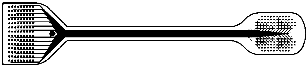
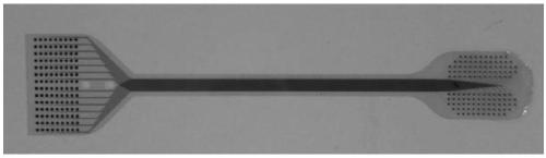
[0059] The struc...

Example Embodiment

[0060] Example 2

[0061] This embodiment provides an implantable microelectrode array, and its preparation method includes the following steps:

[0062] Spin-coat a layer of polyimide (base layer) on the surface of a 4-inch cleaned and dried silicon wafer (base layer), then spin-coat a layer of AZ5214 photoresist on the surface, and expose and develop. Next, a gold layer with a thickness of 120nm was formed by magnetron sputtering, and then the second layer of polyimide was spin-coated and cured. The electrode stimulation sites and pad points were exposed by RIE etching, and the electrodes were separated from the substrate. Released on and off to obtain a 126-channel flexible electrode array.

[0063] The microelectrode array obtained above was treated with vinyl silane on the back of the polyimide (base layer), and gamma rays were used to initiate the copolymerization of caprolactone monomer mixed with black phosphorus and vinyl silane for 30 minutes to achieve chemical gra...

Example Embodiment

[0068] Example 3

[0069] This embodiment provides an implantable microelectrode array, and its preparation method includes the following steps:

[0070] Spin-coat a layer of polyimide with a thickness of 10 μm on the surface of a 4-inch cleaned and dried silicon wafer, then spin-coat a layer of AZ5214 photoresist on the surface, and expose and develop. Next, a platinum layer with a thickness of 120 nm was formed by magnetron sputtering, and then a second layer of polyimide with a thickness of 8 μm was spin-coated and cured. After the electrode sites were exposed by RIE etching, the electrodes were removed from the The substrate was released to obtain a 256-channel flexible electrode array.

[0071] Further, a polyethylene glycol functional layer with a thickness of 100 μm was coated on the back of the electrode.

[0072] The structure of the implanted microelectrode array obtained in this embodiment includes a stimulating end, a lead part and a welding pad end. The stimula...


PUM

PropertyMeasurementUnit
Diameteraaaaaaaaaa
Thicknessaaaaaaaaaa
Thicknessaaaaaaaaaa

Abstract

The invention relates to a functionalized wide-width implanted microelectrode array, a manufacturing method and an application thereof. The functionalized wide-width microelectrode array comprises a functional layer, a base layer, a conducting layer and an insulating layer which are successively arranged. The functional layer is a monomolecular layer, a polymer material layer and/or a polymer compound layer, and has the thickness of 1 nm to 1000 micron. The invention also provides the manufacturing method of the functionalized wide-width implanted microelectrode array. By using the functionalized wide-width microelectrode array, through increasing the size of a microelectrode, a microelectrode bit point, a line, a spacing and other correlation parameters can be effectively adjusted so as to reduce a technology complexity during a microelectrode micro-machining process and greatly increase the yield of a high-cost microelectrode array, and the design problem of a high-density microelectrode array is solved; and through a functionalized wide-width design, a microelectrode array folding or curling function can be realized so as to realize minimally invasive implantation and greatly reduce an operation risk.

Description

technical field [0001] The invention relates to a functional wide-width implanted microelectrode array and a preparation method thereof. Background technique [0002] With the continuous acceleration of the pace of life, because people are often in a state of high physical and mental tension, neurological diseases such as retinitis pigmentosa, macular degeneration, depression, and epilepsy are increasing day by day. At the same time, global aging has exacerbated the probability of neurological diseases and become a major social burden. [0003] The rapid development of wearable or implantable electrical nerve stimulation therapy and the appearance of neural prosthesis have brought new hope to the majority of patients. Nerve electrical stimulation therapy is a method of treatment by regulating nerves without destroying nerve tissue, and it can treat or partially restore nerve function. Due to the safety and effectiveness of this method, for some special neurological disease...

Claims


Application Information

Patent Timeline
IPC IPC(8): A61N1/05C09D4/00C09D105/04C09D105/08C09D167/04C08G63/06C08G63/78
CPCA61N1/0534A61N1/0541A61N1/0543A61N1/056A61N1/0587C08G63/06C08G63/78C09D4/00C09D105/04C09D105/08C09D167/04C08L5/08C08L5/04
Inventor 杜学敏王娟
Owner SHENZHEN INST OF ADVANCED TECH
Why Eureka
Try Eureka