A method for deriving the electrical properties of a mercury cadmium telluride pn junction, and a detector chip

A kind of electrical performance, mercury cadmium telluride technology, applied in the direction of circuits, electrical components, semiconductor devices, etc., can solve the problems of poor response consistency of the detector chip, affecting the effect of electrode ohmic contact, affecting the working voltage, etc., to improve the response Consistency, lifting effect, effect of improving depth uniformity

Active Publication Date: 2021-05-11
北京智创芯源科技有限公司
View PDF9 Cites 0 Cited by
  • Summary
  • Abstract
  • Description
  • Claims
  • Application Information

AI Technical Summary

Problems solved by technology

[0003] In the existing HgCdTe pn junction electrical performance extraction process, the fresh HgCdTe surface obtained after dry etching has strong chemical activity. If the liquid is exposed to the air environment for a long time, it will be oxidized. In addition, during the wet stripping process, the photoresist is easy to remain on the bottom of the etching hole. The above problems may cause the metal and HgCdTe material An additional parasitic resistance is generated at the interface between the electrodes, which affects the effect of the ohmic contact of the electrodes
The parasitic resistance causes the contact resistance of each pixel of the infrared detector to be different. Since the contact resistance has a certain voltage division effect, it will affect the working voltage applied to each pixel. After photoelectric conversion, the output signal of the pixel will be Differences occur, which in turn leads to poor response consistency of the detector chip

Method used


Image

  • A method for deriving the electrical properties of a mercury cadmium telluride pn junction, and a detector chip
  • A method for deriving the electrical properties of a mercury cadmium telluride pn junction, and a detector chip
  • A method for deriving the electrical properties of a mercury cadmium telluride pn junction, and a detector chip

Examples


Embodiment Construction

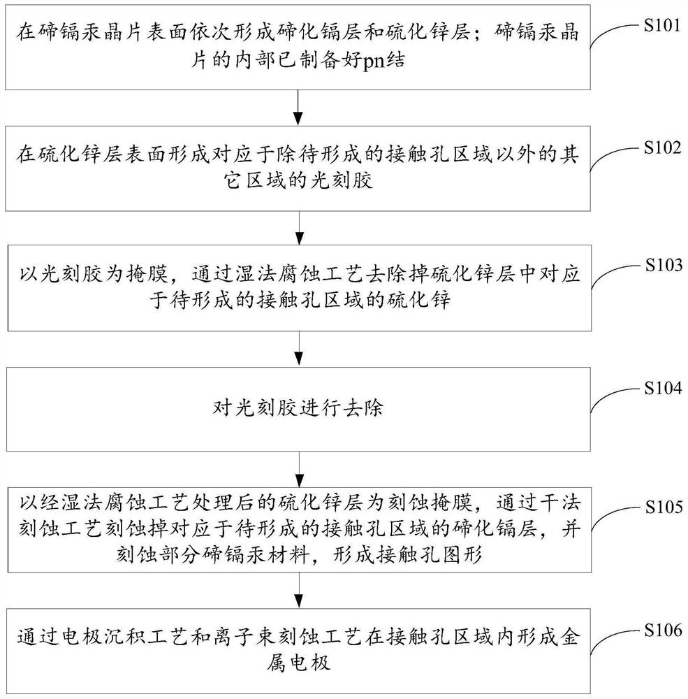
[0032] The following will clearly and completely describe the technical solutions in the embodiments of the present invention with reference to the accompanying drawings in the embodiments of the present invention. Obviously, the described embodiments are only some, not all, embodiments of the present invention. Based on the embodiments of the present invention, all other embodiments obtained by persons of ordinary skill in the art without making creative efforts belong to the protection scope of the present invention.

[0033] The invention provides a method for extracting the electrical properties of the mercury cadmium telluride pn junction, such as figure 1 shown, including the following steps:

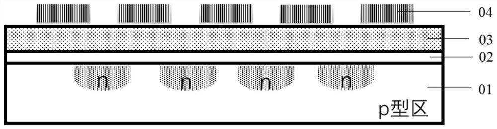
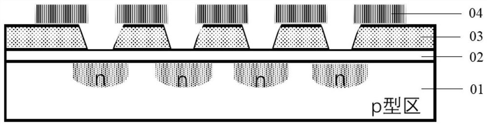
[0034] S101, sequentially forming a cadmium telluride layer and a zinc sulfide layer on the surface of the mercury cadmium telluride wafer; a pn junction has been prepared inside the mercury cadmium telluride wafer;

[0035] It can be understood that the present invention is base...


PUM

PropertyMeasurementUnit
thicknessaaaaaaaaaa
thicknessaaaaaaaaaa

Abstract

This application relates to the technical field of detector chips, and discloses a method for extracting the electrical properties of a mercury cadmium telluride pn junction and a detector chip, including: sequentially forming cadmium telluride on the surface of a mercury cadmium telluride wafer whose pn junction has been prepared inside layer and zinc sulfide layer; form a photoresist corresponding to the area other than the contact hole area to be formed on the surface of the zinc sulfide layer; use the photoresist as a mask, remove the contact corresponding to the contact hole to be formed by a wet etching process Zinc sulfide in the hole area; remove the photoresist; use the zinc sulfide layer treated by the wet etching process as an etching mask, etch the cadmium telluride corresponding to the contact hole area to be formed by a dry etching process layer and part of the HgCdTe material to form a contact hole pattern; and form a metal electrode in the contact hole area through an electrode deposition process and an ion beam etching process. The etching of the contact hole and the deposition of the metal electrode can improve the ohmic contact effect between the HgCdTe material and the metal electrode.

Description

technical field [0001] The invention relates to the technical field of detector chips, in particular to a method for extracting electrical properties of a mercury cadmium telluride pn junction and a detector chip. Background technique [0002] Mercury cadmium telluride is an important material for preparing infrared detectors. Due to its adjustable band gap, the detection spectrum range extends from short-wave bands to very long-wave bands. It has the advantages of high photoelectric detection efficiency and is widely used in early warning detection, infrared Military and civil fields such as reconnaissance and imaging guidance. Detector chip preparation is the core of infrared detection technology. The chip preparation process mainly includes semiconductor device processes such as photolithography, wet chemistry, ion implantation, passivation, electrode preparation, and dry etching. Etching and electrode deposition are two of the device processes. The key link is an import...

Claims


Application Information

Patent Timeline
Patent Type & Authority Patents(China)
IPC IPC(8): H01L31/18H01L21/467H01L31/0224H01L31/103
CPCH01L21/467H01L31/022408H01L31/1032H01L31/1832Y02P70/50
Inventor 不公告发明人
Owner 北京智创芯源科技有限公司
Why Eureka
Try Eureka