Method for preparing near-zero-thickness nanopores by double-sided helium ion beam etching as well as product and application of near-zero-thickness nanopores

A technology of ion beam etching and nanopore, applied in nanotechnology, nanotechnology, nanostructure manufacturing, etc., can solve the problems of insufficient time resolution of nanopores, low capture rate of nanopores, unsuitable for mass production and application, etc.

Pending Publication Date: 2021-01-08
CHONGQING INST OF GREEN & INTELLIGENT TECH CHINESE ACADEMY OF SCI
View PDF0 Cites 4 Cited by
  • Summary
  • Abstract
  • Description
  • Claims
  • Application Information

AI Technical Summary

Problems solved by technology

In addition, in the process of biomolecular sensing, the translocation of DNA and RNA molecules is too fast, and the insufficient time resolution of nanopores is also a big defect.
Some current methods for improving time resolution generally rely on modification or control of experimental conditions, which are not suitable for mass production and application; in addition, some existing nanopore preparation technologies such as dielectric breakdown cannot prepare multiple nanopores with definite positions on the film. Pore ​​structure; and the low capture rate of nanopores is also a big problem

Method used


Image

  • Method for preparing near-zero-thickness nanopores by double-sided helium ion beam etching as well as product and application of near-zero-thickness nanopores
  • Method for preparing near-zero-thickness nanopores by double-sided helium ion beam etching as well as product and application of near-zero-thickness nanopores
  • Method for preparing near-zero-thickness nanopores by double-sided helium ion beam etching as well as product and application of near-zero-thickness nanopores

Examples


example 1

[0040] To prepare near-zero-thickness nanopores with a single-pore structure, the preparation process is specifically carried out according to the following steps:

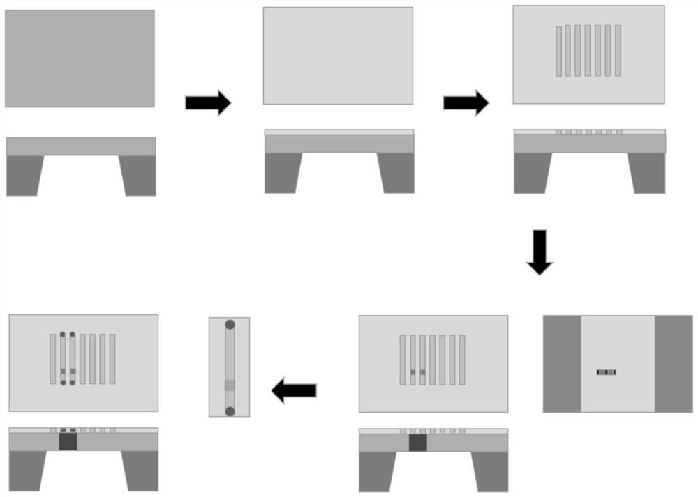
[0041] 1. Select a silicon substrate with a thickness of 10-20 μm, and grow a layer of silicon nitride material with a thickness of 30 nm on the silicon substrate by chemical vapor deposition to obtain a silicon-based film substrate.

[0042] 2. Etching the silicon substrate surface of the silicon-based thin-film substrate by chemical wet etching to form a thin-film window with a side length of 20 μm, that is, to obtain a silicon-based thin-film substrate with a thin-film window.

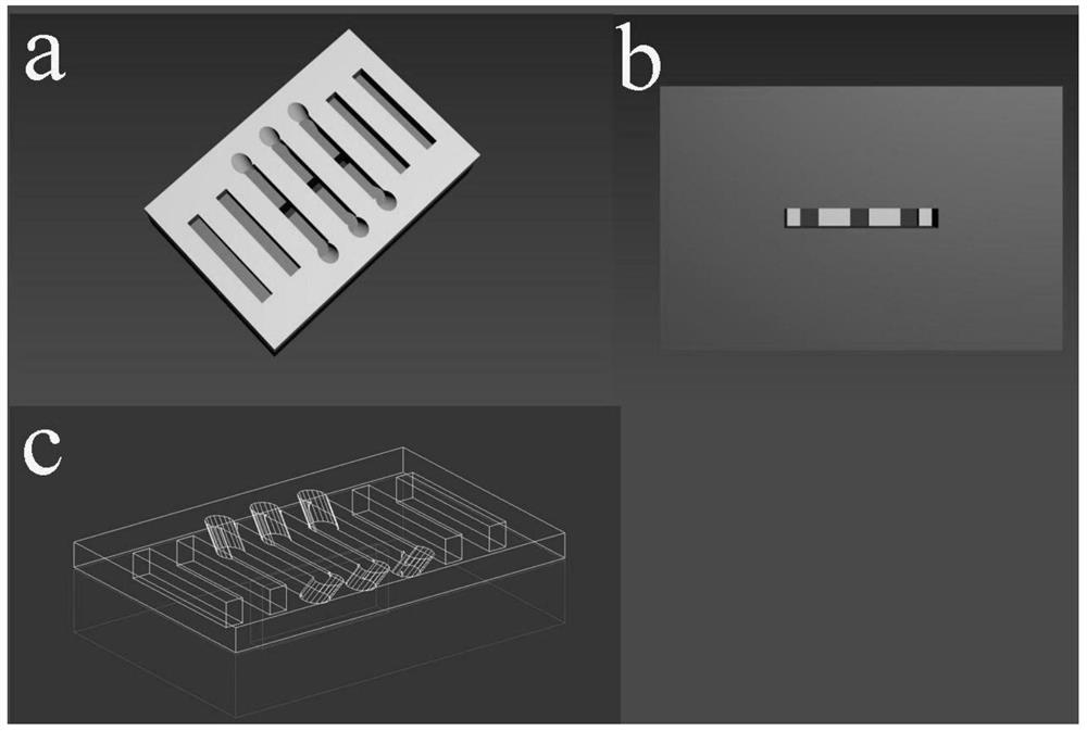
[0043] 3. Use helium ion beam etching on one side (front) of the silicon nitride material (etching parameters are set to: aperture 10μm, beam current less than or equal to 1pA, dose 100-300nc / μm 2 ) to form a row of vertical nanowire arrays with a length of 200nm, a width of 4nm, a depth of 10nm, and a period of 500nm.

[0044] 4. On t...

Embodiment 2

[0049] The preparation process of near-zero-thickness nanopores with double-pore structure is as follows:

[0050] 1. Select a silicon substrate with a thickness of 10-20 μm, first grow a layer of silicon dioxide material with a thickness of 200 nm on the silicon substrate by chemical vapor deposition, and then use chemical vapor deposition to grow a layer of silicon dioxide on the silicon dioxide. A silicon nitride material with a layer thickness of 20nm is obtained to obtain a silicon-based film substrate.

[0051] 2. Etching the silicon substrate surface of the silicon-based thin-film substrate by chemical wet etching to form a thin-film window with a side length of 20 μm, that is, to obtain a silicon-based thin-film substrate with a thin-film window.

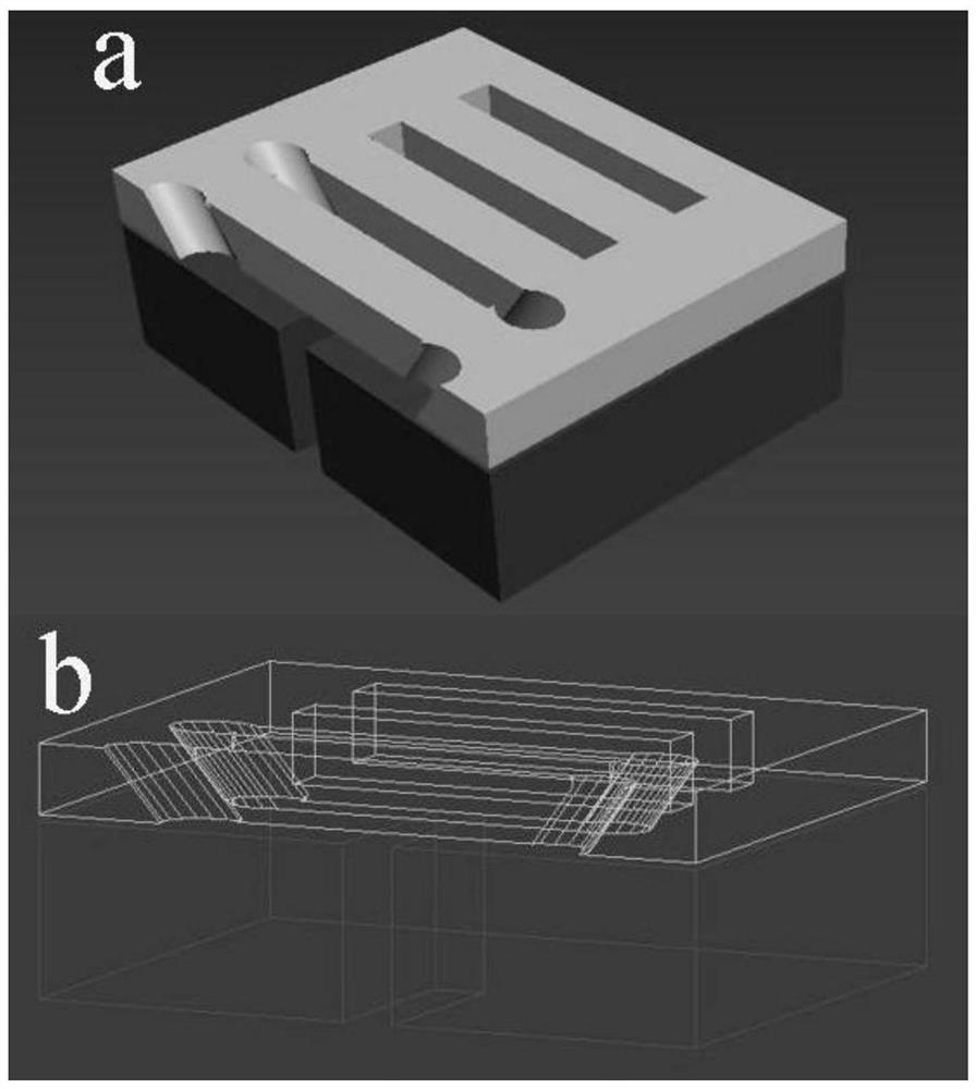
[0052] 3. Use helium ion beam etching on one side (front) of the silicon nitride material (etching parameters are set to: aperture 10μm, beam current less than or equal to 1pA, dose 100-300nc / μm 2 ) to form a row of vertica...

Embodiment 3

[0058] To prepare near-zero thickness nanopores, the preparation process is as follows:

[0059] 1. Select a silicon substrate with a thickness of 10-20 μm, first grow a layer of silicon nitride material with a thickness of 20 nm on the silicon substrate by chemical vapor deposition, and then use chemical vapor deposition to grow a layer of silicon nitride on the silicon nitride. Aluminum oxide material with a layer thickness of 100nm to obtain a silicon-based film substrate.

[0060] 2. Etching the silicon substrate surface of the silicon-based thin-film substrate by chemical wet etching to form a thin-film window with a side length of 20 μm, that is, to obtain a silicon-based thin-film substrate with a thin-film window.

[0061] 3. Use helium ion beam etching on one side (front) of the silicon nitride material (etching parameters are set to: aperture 10μm, beam current less than or equal to 1pA, dose 100-500nc / μm 2 ) for processing (at this time, the choice to process the n...


PUM

PropertyMeasurementUnit
thicknessaaaaaaaaaa
thicknessaaaaaaaaaa
thicknessaaaaaaaaaa

Abstract

The invention relates to a method for preparing near-zero-thickness nanopores by double-sided helium ion beam etching as well as a product and application of the near-zero-thickness nanopores and belongs to the technical field of monomolecular nanopore detection. The invention discloses a method for preparing near-zero-thickness nanopores by double-sided helium ion beam etching. According to the method, a zero-thickness nanopore structure with high controllability is prepared by a helium ion beam processing method with extremely high processing precision and controllability, the material, poresize, pore size pattern and pore size number of the nanopores can be exclusively designed according to the properties of molecules to be detected; the spatial resolution, time resolution and capturerate of the detection of DNA sequences and RNA sequences, DNA sequence modification, RNA sequence modification or protein molecules by the nanopores can be improved.

Description

technical field [0001] The invention belongs to the technical field of single-molecule nanopore detection, and in particular relates to a method for preparing near-zero-thickness nanopores by double-sided helium ion beam etching, as well as products and applications thereof. Background technique [0002] Nanopore single-molecule detection technology is a high-precision biological detection technology based on the Coulter counter principle and ion channel model. In 1953, Coulter proposed that in the electrolyte solution, the basic physical properties of related particles, such as size, shape, charge, etc., could be reflected by monitoring the channel resistance fluctuation caused by particles passing through micron-sized pores. This concept of sensing using resistive pulses has been widely used in the fields of life science and biochemistry research. The sensing principle of nanopores is that when the molecules to be measured, which are approximately the size of the pore dia...

Claims


Application Information

Patent Timeline
Patent Type & Authority Applications(China)
IPC IPC(8): G01N27/00B82B3/00
CPCB82B3/0004G01N27/00
Inventor 王德强刘业香何石轩谢婉谊方绍熙周大明殷博华
Owner CHONGQING INST OF GREEN & INTELLIGENT TECH CHINESE ACADEMY OF SCI
Why Eureka
Try Eureka