

Laminated photonic crystal with optical performance regulation and preparation method thereof
A photonic crystal, optical performance technology, applied in the field of optical materials and photochemistry, can solve the problems of weak adhesion, many defects, easy to fall off, etc., to achieve the effect of bright color, control the number of layers, and simple operation
- Summary
- Abstract
- Description
- Claims
- Application Information
AI Technical Summary
Problems solved by technology
Method used
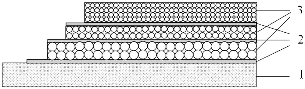
Image

Examples
Embodiment 1
[0030] Step 1: Clean the crystallization dish and glass substrate used in the experiment, and dry them for later use.
[0031] Step 2: Coat a layer of TiO with a thickness of 2-5nm on the glass substrate by spin coating 2 film.
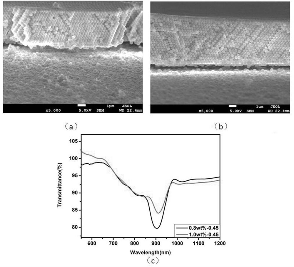
[0032] Step 3: Disperse PMMA colloidal microspheres with a diameter of 401 nm in water to prepare a solution with a concentration of 0.8 wt% (1.0 wt%), place in a crystallization dish and stir for 60 min, and set aside.
[0033] Step 4: Insert the pretreated glass substrate into the above-mentioned crystallization dish containing the 401 nm PMMA colloidal microsphere solution, and place it at a temperature of 40 o C, In a constant temperature and humidity chamber with a humidity of 65%RH, a single-layer photonic crystal film with a single spherical diameter (401 nm) was formed on the substrate by a flow-controlled deposition method.
[0034] Scanning electron microscope (SEM) characterization and ultraviolet-visible transmission spectrum analysis we...
Embodiment 2
[0041] Step 1: Clean the crystallization dish and glass substrate used in the experiment, and dry them for later use.
[0042] Step 2: Coating a layer of TiO with a thickness of 2-5 nm on the glass substrate by spin coating 2 film.
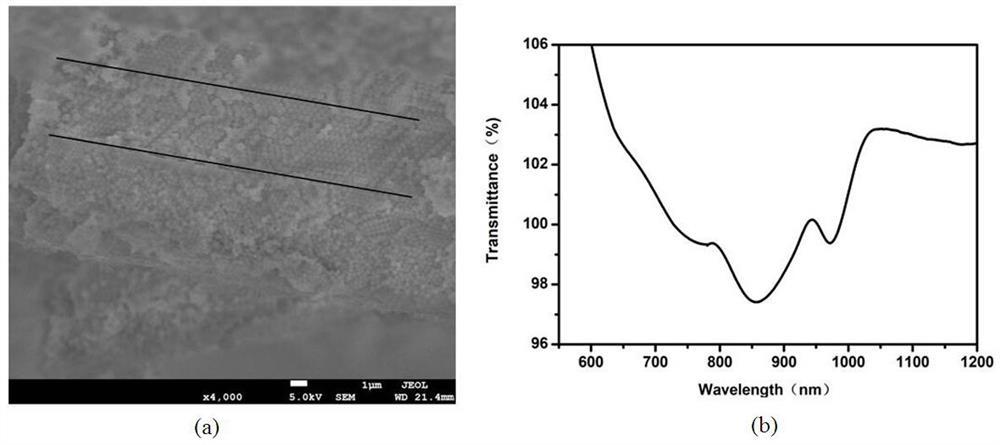
[0043] Step 3: Disperse PMMA colloidal microspheres with a diameter of 318 nm in water to prepare a solution with a concentration of 0.45 wt%, place them in a crystallization dish and stir them for 60 min, and set aside.
[0044] Step 4: Insert the pretreated glass substrate into the above-mentioned crystallization dish containing the 318 nm PMMA colloidal microsphere solution, and place it at a temperature of 40 o C, In a constant temperature and humidity chamber with a humidity of 65%RH, the first layer of unit photonic crystal thin film layer with a single spherical diameter (318 nm) is formed on the substrate by the flow control deposition method.
[0045] Step 5: Disperse PMMA colloidal microspheres with a diameter of 401 nm in water to pre...
Embodiment 3
[0055] Step 1: Clean the crystallization dish and glass substrate used in the experiment, and dry them for later use.
[0056] Step 2: Coating a layer of TiO with a thickness of 2-5 nm on the glass substrate by spin coating 2 film.
[0057] Step 3: Disperse PMMA colloidal microspheres with a diameter of 454 nm in water to form a solution with a concentration of 0.45 wt%, place them in a crystallization dish and stir them for 60 min, and set aside.
[0058] Step 4: Insert the pretreated glass substrate into the above-mentioned crystallization dish containing the 454 nm PMMA colloidal microsphere solution, and place it at a temperature of 40 o C, In a constant temperature and humidity chamber with a humidity of 65% RH, the first layer of unit photonic crystal film layer with a single spherical diameter (454 nm) is formed on the substrate by the flow control deposition method.
[0059] Step 5: Disperse PMMA colloidal microspheres with a diameter of 401 nm in water to prepare a ...
PUM
| Property | Measurement | Unit |
|---|---|---|
| thickness | aaaaa | aaaaa |
| thickness | aaaaa | aaaaa |
| particle diameter | aaaaa | aaaaa |
Abstract
Description
Claims
Application Information