Monocrystalline silicon passivation contact structure and preparation method thereof

A contact structure and monocrystalline silicon technology, which is applied in the fields of final product manufacturing, sustainable manufacturing/processing, semiconductor/solid-state device manufacturing, etc., can solve the problems of poor passivation effect of crystalline silicon, and achieve fast deposition speed and low cost , enhance the collection effect

Active Publication Date: 2021-02-09
ZHEJIANG NORMAL UNIVERSITY
View PDF16 Cites 1 Cited by
  • Summary
  • Abstract
  • Description
  • Claims
  • Application Information

AI Technical Summary

Problems solved by technology

Since the silicon dioxide used as the tunneling layer is usually only 1.0-2.0nm, the heavily doped impurities in the polysilicon will diffuse into the silicon dioxide in the subsequent annealing process of the crystalline silicon cell, resulting in the passivation effect of the silicon dioxide on the crystalline silicon. become worse

Method used


Image

  • Monocrystalline silicon passivation contact structure and preparation method thereof

Examples


Embodiment Construction

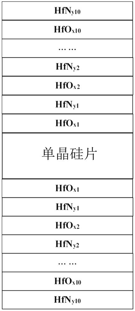
[0027] See attached picture. A schematic diagram of a typical monocrystalline silicon passivation contact structure is shown in figure 1 As shown, 10 layers of HfO were deposited on the front and back of the single crystal silicon wafer respectively x / HfN y , where each layer of HfO x or HfN y The thickness is 3nm, x is the ratio of Hf atoms to O atoms, and y is the ratio of Hf atoms to N atoms. Passivation of composition graded hafnium oxide-hafnium nitride multilayer film / single crystal silicon / composition graded hafnium oxide-hafnium nitride multilayer film prepared by reactive magnetron sputtering method on single crystal silicon substrate contact, in order to reduce defects in the film, followed by annealing at a temperature of 600-700°C. Compared to the tunnel oxide passivation contact, the saturation current density (J 0 ) and contact resistivity (ρ c ) can be significantly reduced.

[0028] The preparation method of the monocrystalline silicon passivation cont...


PUM

PropertyMeasurementUnit
thicknessaaaaaaaaaa
electrical resistivityaaaaaaaaaa
thicknessaaaaaaaaaa

Abstract

The invention discloses a monocrystalline silicon passivation contact structure and a preparation method thereof. The monocrystalline silicon passivation contact structure comprises a monocrystallinesilicon wafer, n layers of HfOx and HfNy are alternately deposited on the front and back surfaces of the monocrystalline silicon wafer, and n is equal to 5-20. The thickness of each layer of HfOx or HfNy is 3nm, wherein the layer closest to the monocrystalline silicon wafer is the first layer, namely HfOx1 and HfNy1, and the layer farthest from the monocrystalline silicon wafer is the n-th layer,namely HfOxn and HfNyn; 2.0 > x1 > x2 >... > x9 > xn > 1.0, and 1.33 > y1 > y2 >... > y9 > yn > 0.67. An HfOx/HfNy multilayer film with gradually changed components is deposited by adopting a reactivemagnetron sputtering method, full-surface passivation and selective contact of monocrystalline silicon are realized, the defects of a tunneling oxide layer passivation contact technology can be overcome, and the monocrystalline silicon passivation contact structure has the advantages of no use of dangerous gas (silane, phosphorane or borane), high deposition speed, low cost and the like.

Description

technical field [0001] The invention belongs to the field of crystalline silicon solar cells, and relates to a monocrystalline silicon passivation contact structure of a hafnium oxide / hafnium nitride multilayer thin film with gradually changing composition, and a preparation method thereof. Background technique [0002] As the minority carrier lifetime of monocrystalline silicon wafers is greatly improved and the thickness is continuously reduced, how to reduce the recombination of carriers on the surface of silicon wafers is the key to further improving the efficiency of crystalline silicon solar cells. Surface passivation can be divided into chemical passivation and field effect passivation. Chemical passivation is usually used to combine the dielectric film with the dangling bonds (uncoordinated silicon atoms) on the silicon surface to reduce the defect density at the interface. . Field effect passivation is to obtain a built-in electric field by doping down the interfac...

Claims


Application Information

Patent Timeline
Patent Type & Authority Applications(China)
IPC IPC(8): H01L31/0216H01L31/18H01L21/02
CPCH01L31/02167H01L31/1804H01L31/1868H01L21/022H01L21/02181H01L21/02266Y02P70/50
Inventor 黄仕华康桥丁月珂李林华
Owner ZHEJIANG NORMAL UNIVERSITY
Why Eureka
Try Eureka