Nano-silver soldering paste, preparation method thereof and application of nano-silver soldering paste in chip packaging interconnection structure
A nano-silver, solder paste technology, applied in welding equipment, welding media, manufacturing tools, etc., can solve the problems of low shear strength and poor compactness, achieve high shear strength, good bonding, and is conducive to large-scale production. The effect of industrial application
- Summary
- Abstract
- Description
- Claims
- Application Information
AI Technical Summary
Problems solved by technology
Method used
Image

Examples
preparation example Construction
[0042] The embodiment of the present invention also provides the preparation method of the nano-silver solder paste as described above, which includes: providing the flaky nano-silver and the organic solvent carrier, stirring the flaky nano-silver and the organic solvent carrier mixing to prepare the nano-silver solder paste.
[0043] In a preferred scheme, the sheet-shaped nano silver is prepared by a liquid phase reduction method. Specifically include the following steps:
[0044] S10, dissolving the reducing agent in the solvent to obtain a first reaction liquid. Wherein, the reducing agent is selected from any one of ascorbic acid, hydrazine hydrate, citrate, polyvinylpyrrolidone, sodium sulfite and sodium borohydride; the solvent is selected from ethanol, ethylene glycol, water, N,N-di Any one of methylformamide, N,N-dimethylacetamide and N-methylpyrrolidone.
[0045]S20, adding the silver source precursor to the first reaction solution, stirring and mixing to form a s...
Embodiment 1
[0054] Dissolve 0.888g of polyvinylpyrrolidone into 200ml of N,N-dimethylformamide, stir and dissolve completely, then add 1.689g of silver nitrate, stir and mix to form a reaction solution. The reaction solution was placed in a reaction kettle, and the reaction time was 4 hours at a temperature of 180°C. After the reaction is finished, it is washed with deionized water, then with ethanol, and finally freeze-dried to prepare and obtain flake nano-silver.
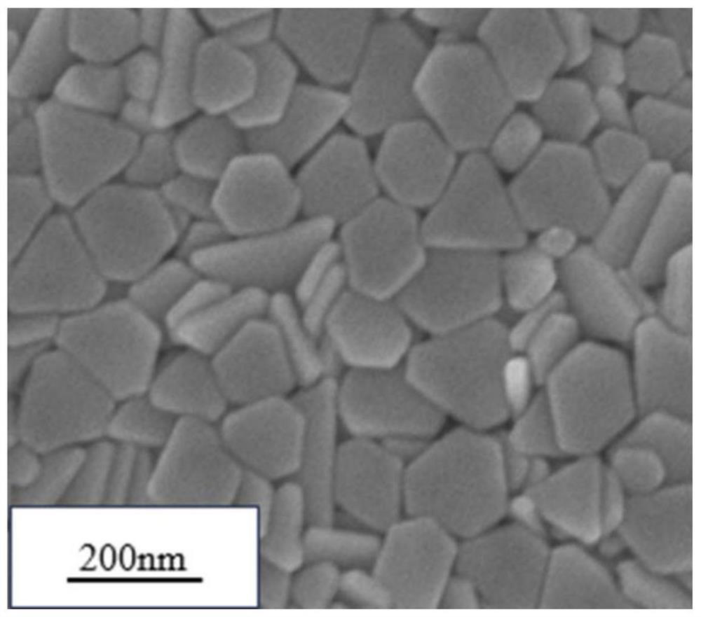
[0055] image 3 It is the SEM figure of the flake nano-silver prepared by the present embodiment, as image 3 As shown, the flaky nano-silver prepared in this embodiment includes triangular flaky nano-silver and hexagonal flaky nano-silver, and the hexagonal flaky nano-silver is relatively more. The particle size range of the flaky nano-silver prepared in this embodiment is 100nm-300nm, and the thickness is 20nm-50nm.
[0056] The prepared flaky nano-silver was mixed with a mixed organic solvent carrier of ethylene glycol...
Embodiment 2
[0066] Dissolve 1.65g of polyvinylpyrrolidone into 200ml of N,N-dimethylacetamide, stir and dissolve completely, add 1.689g of silver nitrate, and stir to form a reaction solution. The reaction solution was placed in a reaction kettle, and the reaction time was 4 hours at a temperature of 180°C. After the reaction is finished, it is washed with deionized water, then with ethanol, and finally freeze-dried to prepare and obtain flake nano-silver.
[0067] Figure 7 It is the SEM figure of the flake nano-silver prepared by the present embodiment, as Figure 7 As shown, the flaky nano-silver prepared in this embodiment includes triangular flaky nano-silver and hexagonal flaky nano-silver, and the triangular flaky nano-silver is relatively more. The particle size range of the flake nano-silver prepared in this embodiment is 100nm-600nm, and the thickness is 20nm-50nm.
[0068] The prepared flaky nano-silver was mixed with a mixed organic solvent carrier of ethylene glycol and β-...
PUM
| Property | Measurement | Unit |
|---|---|---|
| Particle size | aaaaa | aaaaa |
| Thickness | aaaaa | aaaaa |
| Particle size | aaaaa | aaaaa |
Abstract
Description
Claims
Application Information
 - R&D
- Intellectual Property
- Life Sciences
- Materials
- Tech Scout
- Unparalleled Data Quality
- Higher Quality Content
- 60% Fewer Hallucinations
Browse by: Latest US Patents, China's latest patents, Technical Efficacy Thesaurus, Application Domain, Technology Topic, Popular Technical Reports.
© 2025 PatSnap. All rights reserved.Legal|Privacy policy|Modern Slavery Act Transparency Statement|Sitemap|About US| Contact US: help@patsnap.com