Soldering paste and application thereof
A technology of solder paste and nano-silver, which is applied in the field of device welding, can solve the problems of high sintering temperature and low shear strength, and achieve high shear strength, good bonding, and easy-to-achieve process conditions
- Summary
- Abstract
- Description
- Claims
- Application Information
AI Technical Summary
Problems solved by technology
Method used
Image
Examples
Embodiment 1
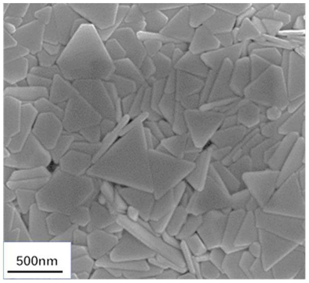
[0037] The flake nano-silver, copper organic source and ethylene glycol were mixed according to a mass ratio of 6:2:1, and stirred and mixed in a mixer for 30 minutes to prepare a solder paste.
[0038] Wherein, the copper organic source is prepared according to the molar ratio of copper hydroxide and ethylenediamine of 1:4 under electromagnetic stirring at room temperature for 30 minutes.
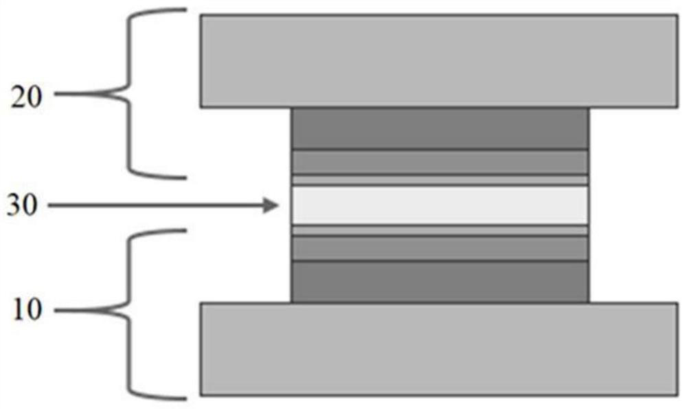
[0039] The solder paste prepared above is applied to the packaging and interconnection structure of the electronic device. Specifically, as attached figure 1 As shown, both the first mother chip 10 and the second mother chip 20 in the package interconnection structure are selected as DBC substrates.
[0040] First, the mother sheets are processed: the DBC substrates (the first mother sheet and the second mother sheet) are ultrasonically washed in ethanol for 3 minutes to remove impurities on the surface, and then dried.
[0041] Next, the solder paste prepared in this embodiment is evenly ...
Embodiment 2
[0046] The flake nano-silver, silver organic source and β-terpineol were mixed according to a mass ratio of 10:4:1, and stirred and mixed in a mixer for 30 minutes to prepare a solder paste.
[0047] The silver organic source is prepared by silver acetate and 2-amino-2-methyl-1-propanol at a molar ratio of 1:4 under electromagnetic stirring at room temperature for 30 minutes.
[0048] The solder paste prepared above is applied to the packaging and interconnection of electronic devices. Specifically, as attached figure 1 As shown, both the first mother chip and the second mother chip in the package interconnection structure are selected as DBC substrates.
[0049] First, the mother sheets are processed: the DBC substrates (the first mother sheet and the second mother sheet) are ultrasonically washed in ethanol for 3 minutes to remove impurities on the surface, and then dried.
[0050] Next, the solder paste prepared in this embodiment is evenly coated on the connection surfac...
Embodiment 3
[0055] Flake nano-silver, copper-silver mixed organic source and organic solvent (ethylene glycol+α-terpineol) were mixed according to the mass ratio of 5:1:1, and stirred and mixed in a mixer for 30min to prepare solder paste.
[0056] The organic source of silver is the product of silver acetate and 2-amino-2-methyl-1-propanol in a molar ratio of 1:4 under electromagnetic stirring at room temperature for 30 minutes. The copper organic source is the product of copper formate and 2-amino-2-methyl-1-propanol molar ratio of 1:4 under electromagnetic stirring at room temperature for 30 minutes. The mixed organic source of copper and silver is formed by mixing the organic source of silver and the organic source of copper according to the mass ratio of 1:1.
[0057] The solder paste prepared above is applied to the packaging and interconnection of electronic devices. Specifically, as attached figure 1 As shown, both the first mother chip and the second mother chip in the package...
PUM
| Property | Measurement | Unit |
|---|---|---|
| particle diameter | aaaaa | aaaaa |
| thickness | aaaaa | aaaaa |
| melting point | aaaaa | aaaaa |
Abstract
Description
Claims
Application Information
 - R&D
- Intellectual Property
- Life Sciences
- Materials
- Tech Scout
- Unparalleled Data Quality
- Higher Quality Content
- 60% Fewer Hallucinations
Browse by: Latest US Patents, China's latest patents, Technical Efficacy Thesaurus, Application Domain, Technology Topic, Popular Technical Reports.
© 2025 PatSnap. All rights reserved.Legal|Privacy policy|Modern Slavery Act Transparency Statement|Sitemap|About US| Contact US: help@patsnap.com


