Preparation method of surface-enhanced Raman scattering substrate

A surface-enhanced Raman and substrate technology, which is applied in Raman scattering, the process for producing decorative surface effects, and the manufacture of microstructure devices, etc. The low probability of hot spot coincidence and the high cost of large-area substrates can achieve the effect of uniform nanostructure and SERS signal, maintaining long-term enhancement ability, and improving overall enhancement ability

Pending Publication Date: 2021-03-16
XI AN JIAOTONG UNIV
View PDF0 Cites 4 Cited by
  • Summary
  • Abstract
  • Description
  • Claims
  • Application Information

AI Technical Summary

Problems solved by technology

Compared with the above two methods, metal nanoparticles on solid substrates have the advantages of low cost, easy large-scale preparation, and high sensitivity, but the uniformity is poor, and the synthesis parameters need to be precisely controlled
Micro-nanofabrication methods can achieve better uniformity, more regular shapes and more ordered arrays, thereby improving the reproducibility of SERS; but it is still difficult to achieve universal testing of analytes of different sizes
Among them, the open hotspots of the nanopyramid SERS substrate have the potential to detect mole

Method used


Image

  • Preparation method of surface-enhanced Raman scattering substrate
  • Preparation method of surface-enhanced Raman scattering substrate
  • Preparation method of surface-enhanced Raman scattering substrate

Examples


preparation example Construction

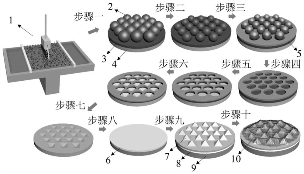
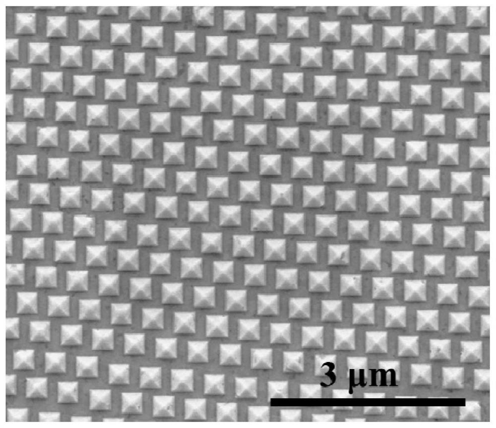
[0043] see figure 1 , a method for preparing a surface-enhanced Raman scattering substrate according to an embodiment of the present invention, comprising the following steps:

[0044] Step 1, in 4 inches of SiO 2 / Si(001) substrate to prepare two-dimensional colloidal crystals with densely packed single-layer nanospheres, and obtain two-dimensional colloidal crystals-SiO 2 / Si(001) substrate sample; SiO 2 The / Si(001) substrate includes a Si layer 4, and SiO disposed on its surface 2 Layer 3.

[0045] Step 2, using plasma etching to reduce the diameter of the nanosphere 2 to obtain the etched two-dimensional colloidal crystal-SiO 2 / Si(001) substrate sample;

[0046] Step 3, use the etched microspheres of the sample in step 2 as a mask, deposit a layer of metal film 5 on the substrate as a mask, and obtain the etched two-dimensional colloidal crystal-metal film mask-SiO 2 / Si(001) substrate sample;

[0047] Step 4, peel off the microsphere 2D colloidal crystal layer in...

Embodiment 1

[0069] A method for preparing a surface-enhanced Raman scattering substrate according to an embodiment of the present invention includes the following steps:

[0070] Step 1, using the Langmuir-Blodgett method on 50nm SiO 2 / Si(001) substrate to prepare a large area of ​​two-dimensional colloidal crystals of close-packed monolayer 500nm polystyrene (PS) microspheres, and obtain two-dimensional colloidal crystals of PS microspheres-SiO 2 / Si substrate sample; wherein the surface of the Si substrate was pre-hydrophilized.

[0071] Step 2, use O 2 As a reaction gas, the diameter of PS microspheres was reduced to 250nm by ICP etching method, and the etched PS microspheres two-dimensional colloidal crystal-SiO 2 / Si substrate samples.

[0072] Step 3, use the etched PS microspheres of the sample in step 2 as a mask, and deposit a layer of Cr on the substrate as a mask by using an electron beam evaporation method to obtain a two-dimensional colloidal crystal-Cr mask of PS microsp...

Embodiment 2

[0083] A method for preparing a surface-enhanced Raman scattering substrate according to an embodiment of the present invention includes the following steps:

[0084] Step 1, using the spin-coating method on 10nm SiO 2 Two-dimensional colloidal crystals of large-area close-packed monolayer 1 μm polymethyl methacrylate (PMMA) microspheres were prepared on Si(001) substrates to obtain two-dimensional colloidal crystals of PMMA microspheres-SiO 2 / Si substrate sample; wherein the surface of the Si substrate was pre-hydrophilized.

[0085] Step 2, use O 2 As a reaction gas, the diameter of PS microspheres was reduced to 800nm ​​by RIE etching method, and the two-dimensional colloidal crystals of PMMA microspheres after etching were obtained-SiO 2 / Si substrate samples.

[0086] Step 3, use the PMMA microspheres after the sample etching in step 2 as a mask, and use an electron beam evaporation method to deposit a layer of Ni on the substrate as a mask to obtain a PMMA microspher...


PUM

PropertyMeasurementUnit
Diameteraaaaaaaaaa
Thicknessaaaaaaaaaa

Abstract

The invention discloses a preparation method of a surface-enhanced Raman scattering substrate. The preparation method comprises the following steps: preparing a densely-arranged single-layer nano microsphere two-dimensional colloidal crystal layer on a SiO2/Si (001) substrate; reducing the diameters of the nano microspheres; depositing a layer of metal film on the surface of the sample; strippingthe microsphere two-dimensional colloidal crystal layer; etching the SiO2 layer by adopting a dry method; etching the Si (001) substrate by adopting a wet method to form an inverted pyramid structure;stripping the SiO2 and the metal mask layer by using an etchant solution to obtain a Si template with an inverted pyramid structure; preparing a noble metal film on the Si template; transferring thenoble metal film to a new substrate by using an adhesive, wherein the pyramid structure is exposed; and transferring a layer of graphene on the surface of the precious metal pyramid. According to themethod disclosed by the invention, the pyramid type SERS substrate is successfully prepared by using two methods of colloid photoetching and micro-nano processing; the prepared substrate is uniform innano pyramid structure distribution in a large-scale range, and has high sensitivity and universality.

Description

technical field [0001] The invention belongs to the technical field of preparation of micro-nano structures, in particular to a preparation method of a surface-enhanced Raman scattering substrate. Background technique [0002] Due to the high sensitivity and unique molecular fingerprint information of surface-enhanced Raman spectroscopy, a large number of related studies have been carried out in recent years. According to the World Health Organization, as of 2015, the top ten causes of death include neurological diseases, diabetes, cardiovascular diseases, cancer and viral diseases. Most diseases start with small changes in the state of the cells, where the altered substances occur in very low concentrations; based on this, surface-enhanced Raman has great advantages in the early detection of diseases. [0003] After decades of development, the application of surface-enhanced Raman scattering (SERS) technology in biosensing and early detection of diseases has made great pro...

Claims


Application Information

Patent Timeline
IPC IPC(8): B81C1/00G01N21/65
CPCB81C1/00031B81C1/00396B81C1/00404G01N21/658B81C2201/0198
Inventor 牛刚武和平任巍赵刚姜陆月赵金燕张易军赵慧丰代立言王哲余雯瑾谢瑱
Owner XI AN JIAOTONG UNIV
Why Eureka
Try Eureka